Difference between revisions of "Introduction to Digital Logic"
| Line 1: | Line 1: | ||
= Objective = | = Objective = | ||
The objective of this lab is to use digital logic to design a combinational logic circuit for an alarm system and to build and test the system using prototyping components. | |||
The objective of this lab is to use | |||
= Overview = | = Overview = | ||
Revision as of 18:21, 28 September 2021
Objective
The objective of this lab is to use digital logic to design a combinational logic circuit for an alarm system and to build and test the system using prototyping components.
Overview
Digital Logic
Digital logic is the conceptual language behind modern computer systems. It uses the Boolean language, which consists of a system of rules that essentially says “yes” or “no” to a series of questions, leading to extremely complicated decisions. The fundamentals of digital logic will be explored in this lab, and a digital logic system will be designed to address a simple problem statement.
Truth Tables
In Boolean logic, there are only two values, true and false, represented by 1 and 0, respectively. These values are combined in equations to yield results that also have these two values. The equations are represented by truth tables that show the inputs to the equation and the outputs produced for those inputs. The rows of the table contain all the combinations of 1s and 0s for the inputs. The number of rows is determined by the number of combinations.
To illustrate a truth table and additional concepts that will be introduced, think of an ATM that has three options: print a statement, withdraw money, or deposit money. The ATM will charge a fee to (1) withdraw money or (2) print a statement without depositing money. The intent of the problem is to develop a Boolean equation and logic circuit that will determine the combinations of actions will result in a fee being charged. First, a truth table should be made for all the combinations of inputs. The inputs are the ATM's three functions. Let variable P stand for printing a statement, W for withdrawing money, and D for depositing money. A “1” indicates the user has taken that action and a “0” indicates the user has not taken that action. There are two outputs -- charge a fee (1) or do not charge a fee (0). The output column will be denoted by C. The truth table in Table 1 shows all the combinations of the inputs and their corresponding outputs.
Table 1: Truth Table for the ATM Example
| Inputs | Output | ||
|---|---|---|---|
| 0 | 0 | 0 | 0 |
| 0 | 0 | 1 | 0 |
| 0 | 1 | 0 | 1 |
| 0 | 1 | 1 | 1 |
| 1 | 0 | 0 | 1 |
| 1 | 0 | 1 | 0 |
| 1 | 1 | 0 | 1 |
| 1 | 1 | 1 | 1 |
Boolean Equations
A truth table is used to write a Boolean equation for a problem. All the combinations that yield an output of 1 are kept, and the equation is written. This is called a Sum of Products solution. Only the combinations that yield an output of 1 are kept because the Boolean equation intends to represent a quantitative function when the output will be true (when a fee is charged in the example of the ATM machine). The combinations that yield an output of 0 are discarded because there is no interest in when the result has a false value. The Boolean equation for the ATM example can be seen in Figure 13.
Figure 13: Boolean Equation
For each of the combinations (rows) resulting in true in Table 1, the terms of the Boolean equation are determined by multiplying the variables together (the AND operation). If an input is true, the variable can be used as-is; for an input that is false, the variable is inverted using the horizontal bar (the NOT operation). Since the output is true if any of the combinations are true, the equation is formed by using addition operations (the OR operation) on all the terms formed by the product of each combination.
Karnaugh Maps (K-Maps)
A truth table showing every combination of inputs and their corresponding outputs yields a Boolean equation that is the solution to a problem in digital logic. This equation can be simplified using a Karnaugh map (K-map). A K-map identifies and eliminates all the conditions that do not contribute to the solution. The resulting simplified Boolean equation is used to build the digital circuit and will be a combination of the logic gates described earlier.
A K-map is a two-dimensional representation of the truth table that shows the common characteristics of the inputs. For an equation with three inputs, usually all the combinations of the first two inputs are shown as four columns and the values for the third input are shown as two rows. For four inputs, all the combinations of the third and fourth inputs are shown as four rows. Only one value can change at a time in adjacent rows or columns. For example, in Table 5, the columns change from 00 to 01 to 11 to 10. Table 5 illustrates the K-map for the ATM example.
| 0 0 | 0 1 | 1 1 | 1 0 | ||
|---|---|---|---|---|---|
| 0 | 0 | 1 | 1 | 1 | |
| 1 | 0 | 1 | 1 | 0 |
Simplified Boolean Equations
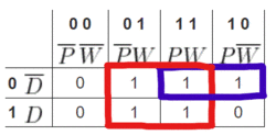
To develop the simplified Boolean equation, look for the cells that have the 1 value in common. Look for cells that can physically be boxed together, where the number of cells in the box is a power of 2 (1, 2, 4, or 8 and so on). The boxes are allowed to overlap so the same cells can be used more than once. Look for the biggest boxes first, and keep finding smaller boxes until all the cells with a 1 in them are used. This means that sometimes just single cells will remain at the end. The cells in the K-map for the ATM example can be grouped like what is shown in Table 6.
In this example, all the cells containing a 1 were covered with two boxes. This means that if the conditions for either box are true, the output will be true. This also means that the simplified Boolean equation will only have two terms. The term for each box can be determined by observing which variables are constant throughout each cell of that box. For the red box, only W remains constant through the four cells. D switches from the top row to the bottom row, and P switches from the left column to the right column. For the blue box, P and remains constant through the two cells, while W switches from the left cell to the right cell. The two boxes yield the simplified Boolean equation shown in Figure 14.
This equation meets the conditions in the truth table in Table 1 and achieves the desired result with the minimum number of logic elements.
Logic Gates
Boolean logic is applied to digital circuitry through the use of simple logic gates. There are symbols for each of these gates, and the connections between them are represented by lines running from the output of one gate to the input of another. A line can connect only one output to each input. There are seven gates: the NOT, AND, OR, NAND, NOR, XOR, and XNOR gates. Only the first three will be used in this lab (Figure 12).
The NOT gate is the simplest of the three. It is an inverter. It has one input and produces its opposite as the output. For example, if a 1 is the input to a NOT gate, a 0 value is outputted, as seen in Table 2. The symbol for the operation is a horizontal bar over the variable. The truth table for a NOT gate is shown in Table 2.
| 0 | 1 |
| 1 | 0 |
The AND gate performs a multiplication operation on its inputs. If all the inputs are true, the output is also true. But if either of the inputs is false, the output is also false. An AND gate can have two or more inputs, but for this lab, it will have two inputs (denoted by A and B in Table 3). The symbol for the AND operation is a dot (·) or the two inputs one after the other with nothing between them. The truth table for an AND gate is shown in Table 3.
| 0 | 0 | 0 |
| 0 | 1 | 0 |
| 1 | 0 | 0 |
| 1 | 1 | 1 |
An OR gate performs an addition operation on its inputs. If either of the inputs is true, the output is also true. But if all the inputs are false, the output is also false. An OR gate can have two or more inputs, but for this lab, it will have two inputs (denoted by A and B in Table 4). The symbol for the OR operation is a plus (+). The truth table for an OR gate is shown in Table 4.
| 0 | 0 | 0 |
| 0 | 1 | 1 |
| 1 | 0 | 1 |
| 1 | 1 | 1 |
Combinational Logic Circuits
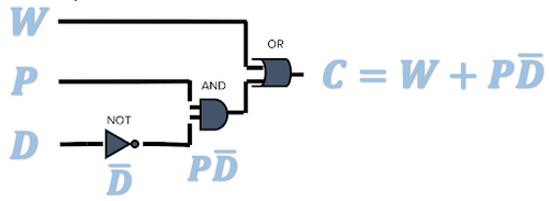
Lastly, a combinational logic circuit can be created using the simplified equation. First, a NOT operation is performed on D by inputting and outputting D through a NOT gate. Then, the P and inverted D are inputted into an AND gate, as denoted by them being multiplied in figure 14. Finally, the result of the AND operation between the P and inverted D and the W is inputted into an OR gate, as denoted by the addition function in figure 14. The final combinational logic circuit can be seen in Figure 15.
Integrated Circuits
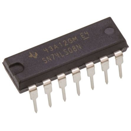
Integrated circuits (IC) can be used to prototype a combinational logic circuit on a breadboard. These devices are small assemblies of electronic components that have been combined into a single unit. In this lab, the IC chips consist of logic gates that can be wired to prototype the logic circuit (Figure 3).
Each chip consists of multiple logic gates. A 7408 chip consists of four AND gates, a 7432 chip consists of four OR gates, and a 7404 chip consists of six NOT gates. These gates can be wired to inputs and outputs to create a combinational logic circuit. The IC chips must also be connected to a power source and ground to operate.
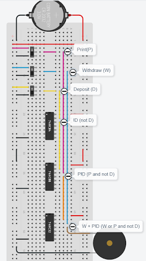
Figure 4 shows how the IC chips can be used to wire the circuit for the ATM problem. In this circuit in Tinkercad, a piezo buzzer represents the output. Slide switches control the Print, Withdraw, and Deposit inputs. The pink wire represents the Print (P) input, the blue wire represents the Withdraw (W) input, and the yellow wire represents the Deposit (D) inputs.
The input is wired to a NOT gate (Chip 7404) to get a output. This is wired to an AND gate input (Chip 7408), along with a input to get a output. This output is wired to an OR gate (Chip 7432), along with a W input to get the final output of .
Materials
- 7432 IC (4 dual-input OR gates)
- 7408 IC (4 dual-input AND gates)
- 7404 IC (6 single-input NOT gates)
- Wires
- 5V Battery Case
- Music Voltmeter
- Slide Switches
Problem Statement
Farmer Georgi owns a 350-acre dairy farm in upstate New York. He sells fresh eggs at the Union Square Greenmarket in Manhattan. It is imperative that Farmer Georgi protects his hen that produces his eggs.
Farmer Georgi has two barns, one hen, and a supply of corn. A fox has been attempting to eat the hen by hiding in one of the two barns. The hen can move freely from one barn to the other. Farmer Georgi sometimes stores corn in one barn and sometimes in the other, but he never stores it in both at the same time. The hen would like to eat the corn and the fox would like to eat the hen. Farmer Georgi needs an alarm system that uses digital logic circuits to protect the hen and the corn. The design should use the fewest logic gates and input variables possible. The alarm should sound if:
- The fox and the hen are in the same barn
- The hen and the corn are in the same barn
Procedure
Step 1. Formulate the Simplified Boolean Equation
- The two barns must be assigned a numeric equivalent before the truth table is prepared. Use 1 for Barn A and 0 for Barn B (1 does not mean true and 0 does not mean false for the inputs). For the alarm output, use 0 to indicate that the alarm should be off, and 1 to indicate that the alarm should be on.
- On a sheet of paper or on the Zoom whiteboard, create a truth table that includes the three inputs (hen, fox, corn) and one output (alarm). Assign the input variables. Use all scenarios for hen, the corn, and the fox. For example, one possible scenario is that the hen, corn and fox are in Barn B, so place a 0 in the three input columns.
- Compute the output column. To do this, analyze the three inputs and logically determine if the alarm will sound in each scenario. Place a 1 in the output column if the alarm will sound and a 0 if it will not.
- Circle all the combinations that produce a 1 in the output column. Create a Boolean equation from this table that uses each of the input combinations that produced a true output. Refer to the Overview section if there is any confusion.
- Create a K-map. Draw a map that uses all the combinations from the Boolean equation. Use the Boolean equation to fill in the 1s and 0s on the K-map.
- Box the pairs of 1s. The 1s may only be boxed in powers of 2 starting with the largest possible combination and working down to the smallest. The outcomes that do not contribute to the solution are to be discarded.
- This process yields a simplified Boolean equation. Write this simplified Boolean equation down.
- Draw a combinational logic circuit of the simplified Boolean equation.
- Have a TA approve the steps to obtain the combinational logic circuit.
Step 2. Test the Integrated Circuits (ICs)
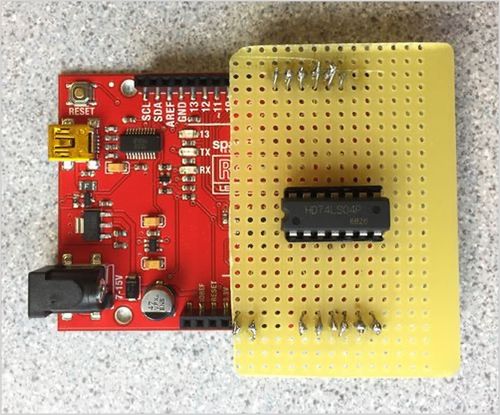
Before building the circuit, the ICs used in wiring the alarm system must be tested to determine if they are functioning. If the procedure is completed without verifying that the ICs work, it will require additional time and troubleshooting in Step 3. The system for checking the ICs uses an Arduino board to send and receive signals from the AND/OR/NOT chips and determines if they are functioning properly.
Load the chip onto the Arduino board (Figure 5 ) and start the Serial Monitor on the Arduino program (top right corner). The code will cycle through the basic inputs (0, 1 for NOT; 00, 01, 10, 11 for AND/OR) and then send the outputs of each gate in the chip back to the Arduino board. The code compares those results to the expected result. It displays each input/output pair and the final result. After the test is done, carefully remove the chips from the test station.
Step 3. Build the Combinational Logic Circuit
- Obtain a pre-assembled breadboard from the TA.
- Build the circuit on a pre-assembled breadboard. On the board, identify each of the three IC chips as an AND, OR, or NOT gate. To do this, read the number on the chip and match it with the numbers shown in Figure 7. Look for the notch at one end of each chip to orient the chip to the diagrams in Figure 7 and to match the pins.
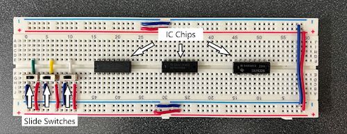
- Place the IC chips over the bridge in the breadboard with the NOT chip on top, the AND chip in the middle, and the OR chip at the end (Figure 8).
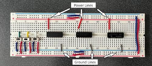
- Power the chips by inserting one end of an electrical lead into the power column marked + on the breadboard. Insert the other end of the lead into Pin 14 of the IC chip. Repeat this process for all three chips.
- Ground the chips by inserting one end of another electrical lead into the ground column marked – on the breadboard and the other end into Pin 7 of the IC chip. Repeat this process for all three chips (Figure 9).
- Look at the top right corner of the breadboard to find the rows for each input. Wire Row 5 to use as the fox input variable and begin wiring the circuit based on the simplified Boolean equation. Repeat this using Row 10 for the hen input and Row 15 for the corn input.
- Continue this process until the entire circuit is wired. Insert one end of a wire into the final output of the logic circuit. Attach the other end of the wire to the last row on the breadboard (Row 61).
- Once the logic circuit is complete, it must be approved by a TA before it can be tested. If the circuit is approved, the TA will provide and wire a battery to power the circuit, and a music voltmeter to represent the alarm. The battery will be wired to the power and ground rails on the breadboard, and the music voltmeter will be wired to the output set up in Step 8. Power the circuit by toggling the switches on the back of the battery case.
- Operate the slide switches corresponding to the corn, fox, and hen. Observe the music voltmeter to see if the alarm goes off based on the inputs to each barn. Compare the results to the truth table to determine if the circuit is operating correctly.
- If the circuit is operating correctly, take pictures of the circuit and clean up the workspace.
- If the circuit is not operating properly, disconnect the circuit from power and examine the circuit including wiring issues.
The lab work is now complete. Refer to the Assignment section for the instructions to prepare the lab report.
Assignment
Individual Lab Report
Follow the lab report guidelines laid out in the EG1004 Writing Style Guide in the Technical Writing section of the manual. Use the outline below to write this report.
- Describe the problem statement regarding Farmer Georgi
- Describe how AND, OR, and NOT gates work
- What is a truth table? Explain the process for obtaining a Boolean equation from a truth table
- What is a K-map? How does it contribute to obtaining a simplified Boolean equation? To demonstrate simplification, show what the equation would look like if terms were written for each of the true values and the simplified equation by applying the K-map. Discuss how much simpler the circuitry is as a result of applying the K-map
- Include the truth table, Boolean equation, K-map, simplified Boolean equation, and combinational logic circuit developed during the lab
- Describe how to construct a digital logic circuit using Boolean equations, K-maps, truth table
- Why is there a need for the minimization of a logic design and what are the advantages?
- How does the use of a combinational logic circuit contribute to advances in technology?
- Describe how the final combinational logic circuit was obtained
- Discuss other possible design/procedural improvements
- Contribution Statement
Team Powerpoint Presentation
Follow the presentation guidelines laid out in the EG1004 Lab Presentation Format in the Technical Presentations section of the manual. When preparing the presentation, consider the following points.
- How does digital logic impact the world today?
- Looking into the future, how will digital logic change the world?
- Include the truth table, Boolean equation, K-map, simplified Boolean equation, and combinational logic circuit developed during the lab
References
Boole, George, Encyclopedia Britannica, 2003. Encyclopedia Britannica Online. Retrieved July 29, 2003 http://www.britannica.com/eb/article?eu=82823
| ||||||||




 output. This is wired to an AND gate input (Chip 7408), along with a
  output. This output is wired to an OR gate (Chip 7432), along with a W input to get the final output of
  .
.
