Difference between revisions of "Introduction to Digital Logic"
| (67 intermediate revisions by 9 users not shown) | |||
| Line 1: | Line 1: | ||
= Objective = | = Objective = | ||
The objectives of this lab are to design, build, and test an alarm system using digital logic. | |||
The | |||
= Overview = | = Overview = | ||
In this lab, the task is to create an alarm system for a client named Farmer Georgi. Farmer Georgi owns a 350-acre dairy farm in upstate New York. He sells fresh eggs at the Union Square Greenmarket in Manhattan. It is imperative that Farmer Georgi protects his hen that produces his eggs. | |||
Farmer Georgi has two barns, one hen, and a supply of grain. A fox has been attempting to eat the hen by hiding in one of the two barns. The hen can move freely from one barn to the other. Farmer Georgi sometimes stores grain in one barn and sometimes in the other, but he never stores it in both at the same time. The hen would like to eat the grain and the fox would like to eat the hen. Farmer Georgi needs an alarm system that uses digital logic circuits to protect the hen and the grain. The design should use the fewest logic gates and input variables possible. The alarm should sound if: | |||
* The fox and the hen are in the same barn | |||
* The hen and the grain are in the same barn | |||
== Digital Logic == | |||
Construction of the alarm system will require the application of digital logic. <b>Digital logic</b> is the conceptual language behind modern computer systems. It is based on Boolean algebra that originally used two values, true and false, to design and solve logic problems. In its modern form, this logic uses true and false, HIGH and LOW, positive and negative,1 and 0, and other binary values to design and operate complex digital systems. 1 and 0 will be used exclusively in this exercise. The fundamentals of digital logic will be explored in this lab by designing a digital logic system to address a simple problem statement. | |||
=== Truth Tables === | |||
In Boolean algebra, results can either be true (usually denoted as 1) or false (usually denoted as 0). Logical operators can be used to construct relationships, known as Boolean equations, between variables in a dataset. There are seven Boolean operators, but only three – AND, OR, and NOT – are used in this lab. | |||
The AND operator confirms that two or more Boolean expressions are 1. The OR operator confirms that either one condition or another is 1. The NOT operator confirms if a value is 0. | |||
Constructing a Boolean equation begins with the creation of a '''truth table''', which represents the inputs and outputs of an operation. | |||
Consider the following example: | |||
Any combination of three tasks can be performed by an ATM: to print a statement (P), to withdraw money (W), or to deposit money (D). The ATM will charge a fee (C) to either withdraw money or print a statement without depositing money. A truth table can be constructed to describe when a fee will be charged (Table 1). Let 1 indicate that the user has taken that action and 0 indicate that the user has not taken that action. | |||
<center> | <center> | ||
| Line 93: | Line 52: | ||
|} | |} | ||
</center> | </center> | ||
All combinations of actions must be considered.This represents the inputs of the truth table. | |||
Consider the results of these actions, or the output of the table. The output of this truth table is determined by the designer. By considering each input or combination of inputs, an output for each row is found. For example, the input PDW = 000 on row 1 represents that no statement was printed, no money was withdrawn, and no money was deposited. As a fee is only charged when money is withdrawn (W = 1), or a statement is printed without depositing money (P = 1 and D = 0), this combination of inputs will result in no fee being charged. This is 0 for the output on the truth table, as shown in row 1. Continuing down the table and filling each row by logically considering the inputs and the output, the truth table will then show all inputs and their output. | |||
=== Boolean Equations === | |||
The truth table is used to write the Boolean equation for the problem. The Boolean equation is a representation of when the output is 1. In the ATM example, a Boolean equation is written using the 1 outputs or when a fee is charged. | |||
For each of the input combinations (rows) in truth table that output 1, the terms of the Boolean equation are determined by multiplying the variables together (the AND operation). If an input is 1, the variable can be used as-is; for an input that is 0, the variable is inverted using a macron or an overbar (the NOT operation) above the variable. Since the output is 1 if any of the combinations are 1, the equation is formed by using addition operations (the OR operation) on all the terms formed by the product of each combination, which is called a Sum of Products solution. But using this equation will create a design that is complex and has redundant components.Equation 1, below, is the Boolean equation for the ATM example detailed above. | |||
<center><math>C = \overline{P} W \overline{D} + \overline{P} W D + P \overline{W}\,\overline{D} + P W \overline{D} + P W D\,</math></center> | |||
<p style="text-align:right">(1)</p> | |||
=== Karnaugh Maps === | |||
Boolean equations can be simplified using a Karnaugh map (K-map). A K-map identifies and eliminates all of the conditions that do not contribute to the solution. The resulting simplified Boolean equation is used to build the digital circuit and will be a combination of the logic gates. | |||
A K-map is a two-dimensional representation of the truth table that shows the common characteristics of the inputs. For an equation with three inputs, usually all the combinations of the first two inputs are shown as four columns and the values for the third input are shown as two rows. For four inputs, all the combinations of the third and fourth inputs are shown as four rows. Only one value can change at a time in adjacent rows or columns. For example, in Table 2, the columns change from 00 to 01 to 11 to 10, where only 1 variable changes at a time between adjacent columns. Each cell is filled by looking at the row and column of the cell, finding the row on the truth table, and then writing the output of the truth table onto the K-map. For example, for the cell highlighted in blue, the row and column says <math>\overline{D}\,</math> and <math>\overline{P} \, \overline{W}\,</math>, respectively. On the truth table with the inputs PDW = 000, the output is 0, and that is used to fill the cell. This is repeated for every cell in the K-map. Table 2 is the K-map for the ATM example. | |||
<center> Table 2: K-Map for the ATM Example | |||
{| class="kmap" | |||
|- | |||
!!!!!0 0!!0 1!!1 1!!1 0 | |||
|- | |||
!!!!!<math>\overline{P} \, \overline{W}\,</math>!!<math>\overline{P} W</math>!!<math>P W\,</math>!!<math>P \overline{W}</math> | |||
|- | |||
!0!!<math>\overline{D}\,</math> | |||
|0||1||1||1 | |||
|- | |||
!1!!<math>D\,</math> | |||
|0||1||1||0 | |||
|- | |||
|} | |||
</center> | |||
=== Simplified Boolean Equations === | |||
To develop the <b>simplified Boolean equation</b>, look for all the cells with a 1 that can physically be boxed together, where the number of cells in the box is a power of 2 (1, 2, 4, or 8 and so on). The boxes are allowed to overlap so the same cells can be used more than once. Look for the biggest boxes first, and keep finding smaller boxes until all the cells with a 1 in them are used. This means that sometimes just single cells will remain at the end. The cells in the K-map for the ATM example can be grouped as shown in Table 3. | |||
<center>Table 3: K-Map Boxes for the ATM Example</center><br> | |||
[[Image:Kmap_Boxes.gif|250px|center]] | |||
In this example, all the cells containing a 1 were covered with two boxes. This means that if the conditions for either box are 1, the output will be 1. This also means that the simplified Boolean equation will only have two terms. The term for each box can be determined by finding the variables that are constant throughout each cell of that box. For the red box, only W remains constant through the four cells. D switches from the top row to the bottom row, and P switches from the left column to the right column. This means that even though D switches between 0 and 1, and P switches between 0 and 1, the output remains constant. They are irrelevant in determining the output, and only the constant term, W, is relevant for determining the output highlighted by the red box. For the blue box, P and <math>\overline{D}\,</math> remains constant through the two cells, while W switches from the left cell to the right cell, meaning that <math>\overline{P} \, \overline{D}\,</math> is responsible for determining the output of the blue box, and W is irrelevant. The relevant terms for each box are added to produce the simplified Boolean equation shown in (3). | |||
<center><math>C = W + P\overline{D}\,</math></center> | |||
<p style="text-align:right">(3)</p> | |||
This equation meets the conditions in the truth table and achieves the desired result with the minimum number of logic elements. | |||
=== Logic Gates === | === Logic Gates === | ||
Digital logic is applied to digital circuitry through the use of simple '''logic gates'''. There are symbols for each of these gates, and the connections between them are represented by lines running from the output of one gate to the input of another. A line can connect only one output to each input. There are seven gates, but only the NOT, AND and OR gates will be used in this lab (Figure 1). | |||
[[Image: | [[Image:ICchips.jpg|500px|thumb|center|Figure 1: Logic Gate Symbols]] | ||
The <b>NOT gate</b> | The <b>NOT gate</b> is an inverter. It has one input and produces its opposite as the output. For example, if a 1 is the input to a NOT gate, a 0 is outputted, as seen in Table 4. The symbol for the operation is a macron or over bar over the variable. The truth table for a NOT gate is shown in Table 4. | ||
<center> Table | <center> Table 4: Truth Table for a NOT Gate | ||
{| class="truthtable" | {| class="truthtable" | ||
|- | |- | ||
| Line 114: | Line 123: | ||
</center> | </center> | ||
The <b>AND</b> gate performs a | The <b>AND</b> gate performs a comparison operation on its inputs. If all the inputs are 1, the output is also 1. If either of the inputs is 0, the output is also 0. An AND gate can have two or more inputs (denoted by A and B in Table 5), but two inputs were used in this exercise. The symbol for the AND operation is a dot (·) between the variables , and is represented by multiplication mathematically. The truth table for an AND gate is shown in Table 5. | ||
<center>Table | <center>Table 5: Truth Table for an AND Gate | ||
{| class="truthtable" | {| class="truthtable" | ||
|- | |- | ||
| Line 132: | Line 141: | ||
</center> | </center> | ||
An <b>OR</b> gate performs | An <b>OR</b> gate performs a comparison operation on its inputs. If either of the inputs is 1, the output is also 1. But if all the inputs are 0, the output is also 0. An OR gate can have two or more inputs, but for this lab, it will have two inputs (denoted by A and B in Table 6). The symbol for the OR operation is a plus (+), and is represented by addition mathematically. The truth table for an OR gate is shown in Table 6. | ||
<center>Table | <center>Table 6: Truth Table for an OR Gate | ||
{| class="truthtable" | {| class="truthtable" | ||
|- | |- | ||
| Line 150: | Line 159: | ||
</center> | </center> | ||
=== | === Combinational Logic Circuits === | ||
A '''combinational logic circuit''' can be created using the simplified equation. A combinational logic circuit is a combination of logic gates that takes in inputs and produces an output according to a truth table or Boolean equation. For the ATM circuit, a NOT operation is performed on <math>D</math> by inputting and outputting <math>\overline{D}\,</math> through a NOT gate. <math>P</math> and <math>\overline{D}\,</math> are inputted into an AND gate, as denoted by them being multiplied in the simplified Boolean equation.The result of the AND operation between the <math>P</math> and <math>\overline{D}\,</math> and the W is inputted into an OR gate, as denoted by the addition function in the Boolean simplified equation. The final combinational logic circuit can be seen in Figure 2. | |||
[[Image:CombinationalCircuit.jpg|500px|thumb|center|Figure 2: Combinational Logic Circuit for ATM Example]] | |||
=== Integrated Circuits === | |||
<b>Integrated circuits (IC)</b> can be used to prototype a combinational logic circuit on a breadboard. These devices are small assemblies of electronic components that have been combined into a single unit. In this lab, the IC chips consist of logic gates that can be wired to prototype the logic circuit (Figure 3). For IC chips and other electrical components, power (5V) and ground (0V) represent 1 and 0, respectively. | |||
[[Image:Lab_ICChip.jpg|500px|thumb|center|Figure 3: An IC Chip]] | |||
Each chip consists of multiple logic gates. A 7408 chip consists of four AND gates, a 7432 chip consists of four OR gates, and a 7404 chip consists of six NOT gates. These gates can be wired to inputs and outputs to create a combinational logic circuit. The IC chips must also be connected to a power source and ground to operate. | |||
Figure 4 shows how the IC chips can be used to wire the circuit for the ATM problem. In this circuit in Tinkercad, a piezo buzzer represents the output. Slide switches control the Print, Withdraw, and Deposit inputs, where connecting the switch to the power sets the input to 1, and connecting the switch to the ground sets the input to 0. The pink wire represents the Print (P) input, the blue wire represents the Withdraw (W) input, and the yellow wire represents the Deposit (D) inputs. | |||
[[Image:Lab_ICBreadboard.jpg|500px|thumb|center|Figure 4: The ATM Problem Prototyped on a Breadboard Using IC Chips]] | |||
The <math>D</math> input is wired to a NOT gate (IC 7404) to get a <math>\overline{D}</math> output. This output is wired to an AND gate input (IC 7408), along with a <math>P</math> input to get a <math>P\overline{D}</math> output. This output is wired to an OR gate (IC 7432), along with a W input to get the final output of <math>W+ P\overline{D}</math>. | |||
In this lab exercise, these steps will be applied to construct the alarm requested by Farmer Georgi. | |||
[[Image: | == Basic Breadboard Wiring == | ||
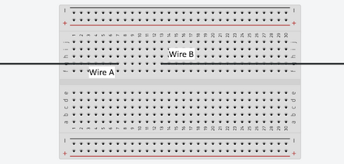
'''Wire A''' and '''Wire B''' are not connected (Figure 5). | |||
[[Image:Wire_A_and_B.png|500px|thumb|center|Figure 5: Wire A and Wire B Sample Connection]] | |||
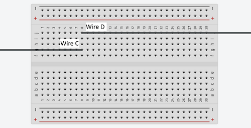
'''Wire C''' and '''Wire D''' are connected together (Figure 6). | |||
[[Image:Wire_C_and_Wire_D.png|500px|thumb|center|Figure 6: Wire C and Wire D Sample Connection]] | |||
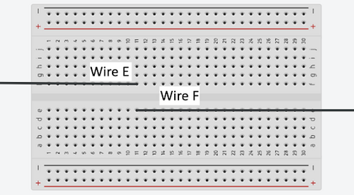
'''Wire E''' and '''Wire F''' are not connected (Figure 7). | |||
[[Image:Wire_E_and_Wire_F.png|500px|thumb|center|Figure 7: Wire E and Wire F Sample Connection]] | |||
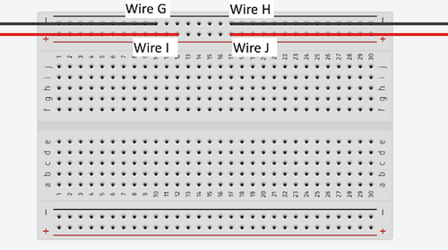
'''Wire G''' and '''Wire H''' are connected (to be grounded) together. | |||
'''Wire I''' and '''Wire J''' are connected (to be powered) together (Figure 8). | |||
[[Image:Wire_GH_and_Wire_IJ.png|500px|thumb|center|Figure 8: Wires G&H and Wires I&J Sample Connections]] | |||
An example of one of the AND gated connected with inputs and outputs for that gate shown (Figure 9). Refer to Figure 1 to see all possible inputs and outputs on an IC chip. | |||
[[Image:And_Gate_Breadboard.png|500px|thumb|center|Figure 9: AND Gate Example]] | |||
Sample connection for an LED with 220 Ω resistor (Figure 10). | |||
[[Image:Led_Resistor.png|500px|thumb|center|Figure 10: LED with Resistor Sample Connection]] | |||
= Materials = | = Materials = | ||
* 7432 IC (four dual-input OR gates) | |||
* 7408 IC (four dual-input AND gates) | |||
* 7404 IC (six single-input NOT gates) | |||
* Pre-Assembled Breadboard | |||
* Wires | |||
* | * 5V Battery Case | ||
* LED | |||
* | * 220 Ω Resistor | ||
* | * Slide Switches | ||
* | |||
* | |||
= Procedure = | = Procedure = | ||
== | === Step 1. Formulate the Simplified Boolean Equation === | ||
== | |||
# The two barns must be assigned a numeric equivalent before the truth table is prepared. Use 1 to represent that a variable (hen, fox, or grain) is in Barn A and 0 to represent that the variable is in Barn B. For the alarm output, use 0 to indicate that the alarm should be off, and 1 to indicate that the alarm should be on. When building the circuit, 1 is power and 0 is ground. | |||
# On a sheet of paper, create a truth table that includes the three inputs (hen, fox, grain) and one output (alarm). Assign the input variables. Use all scenarios for hen, the grain, and the fox. For example, one possible scenario is that the hen, grain and fox are in Barn A, so place a 1 in the three input columns. The number of rows in the truth table should be 2^n where n is the number of inputs. | |||
# Compute the output column. Analyze the three inputs and determine if the alarm will sound for each combination. Place a 1 in the output column if the alarm will sound and a 0 if it will not. | |||
# Circle all the combinations that produce a 1 in the output column. Create the Boolean equation from this table that uses each of the input combinations that produced a 1 output. Refer to the Overview section if there is any confusion. | |||
# Draw a K-map and fill the cells in using the truth table as discussed in the Overview. | |||
# Box the groups of 1s. The 1s may only be boxed in powers of 2. Start with the largest box, and continue to the smallest, making sure to box each cell containing a 1, and also making sure to have as few boxes as possible. Once all the boxes are drawn, identify the constant variables for each box to create the simplified Boolean equation. | |||
# Draw a combinational logic circuit of the simplified Boolean equation. Use a light bulb to represent the alarm. EG1004 recommends using [https://logic.ly/demo/ logic.ly] for creating the combinational logic circuit. Screenshot the circuit instead of saving it. | |||
# Have a TA approve the combinational logic circuit. | |||
=== | === Step 2. Test the Integrated Circuits (ICs) === | ||
'''This step will be done by the lab TAs. Read the following explanation for Step 2 and let the lab TAs know when the ICs are ready to test.''' | |||
Before building the circuit, the ICs used in wiring the alarm system must be tested to determine if they are functioning. If the procedure is completed without verifying that the ICs work, it will require additional time and troubleshooting when the alarm circuit is built. The system for checking the ICs uses an Arduino board to send and receive signals from the AND/OR/NOT chips and determines if they are functioning properly. | |||
Load the chip onto the Arduino board (Figure 11) and start the Serial Monitor on the Arduino program (top right corner). The code will cycle through the basic inputs (0, 1 for NOT; 00, 01, 10, 11 for AND/OR) and then send the outputs of each gate in the chip back to the Arduino board. The code compares those results to the expected result. It displays each input/output pair and the final result. After the test is done, carefully remove the chips from the test station. | |||
[[Image:ICtesting.jpg|500px|thumb|center|Figure 11: IC Testing Setup]] | |||
=== Step 3. Build the Combinational Logic Circuit === | |||
# Obtain a pre-assembled breadboard from the TA. | |||
# Build the circuit on a pre-assembled breadboard. On the board, identify each of the three IC chips as an AND, OR, or NOT gate. To do this, read the number on the chip and match it with the numbers shown in Figure 12. <b>Look for the notch at one end of each chip to orient the chip to the diagrams in Figure 12 and to match the pins</b>. Note that each IC chip has multiple gates. [[Image:ICchips.jpg|500px|thumb|center|Figure 12: IC Numbers and Pins]] | |||
# Place the IC chips over the bridge in the breadboard with the NOT chip on top, the AND chip in the middle, and the OR chip at the end (Figure 13). Remember to orient the IC chips using the notch. [[Image:ICbreadboard.jpg|500px|thumb|center|Figure 13: IC Chip in Breadboard]] | |||
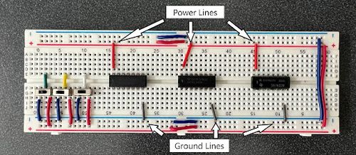
# Power the chips by inserting one end of an electrical lead into the power column marked + on the breadboard. Insert the other end of the lead into Pin 14 of the IC chip. Refer to Figure 7 for the pin numbers on each IC chip. Repeat this process for all three chips. | |||
# Ground the chips by inserting one end of another electrical lead into the ground column marked – on the breadboard and the other end into Pin 7 of the IC chip. Repeat this process for all three chips (Figure 14).[[Image:ICPower.jpg|500px|thumb|center|Figure 14: IC Chips Connected to Power and Ground]] | |||
# Using three switches on the breadboard, assign each switch to an input variable (fox, grain, hen). For all three switches, the wire connected to the ground represents Barn A, and the wire connected to power represents Barn B. | |||
# The center leads from each switch begins the wiring for each input variable. Follow Figure 12 to connect to the inputs and outputs of each gate on the IC chip. | |||
# Continue this process until the entire circuit is wired according to the simplified Boolean equation. Insert one end of a wire into the final output of the logic circuit (This will most likely be the output of an OR gate). Attach the other end of the wire to the last row of the breadboard where no other connections are made. This will serve as the connection for the power side of the LED. The LED must also be grounded. '''Ensure that a 220 Ω resistor is added connecting the negative terminal of the LED and ground.''' | |||
# Have a TA verify and approve the wiring before supplying any power to the circuit. | |||
# Ensure the 5 V Battery is powered off. Wire the positive (red) wire to the power line of the breadboard. Repeat this process for the ground (black) wire, and wire it to the ground power line of the breadboard. These wires will serve as the power and ground for all the IC chips and the slide switches. Power the battery and observe the LED. | |||
# Operate the slide switches corresponding to the fox, grain, and hen. Observe the LED to see if the alarm goes off based on the inputs to each barn. Compare the results to the truth table to determine if the circuit is operating correctly. | |||
# If the circuit is not operating properly, disconnect the circuit from power and examine the circuit including the wiring. | |||
# If the circuit is operating correctly, take pictures of the circuit and clean up the workspace. | |||
The lab work is now complete. Refer to the Assignment section for the instructions to prepare the lab report. | The lab work is now complete. Refer to the Assignment section for the instructions to prepare the lab report. | ||
= Assignment = | = Assignment = | ||
== | == Individual Lab Report == | ||
{{Labs:Lab Report}} | {{Labs:Lab Report}} | ||
* Abstract | |||
* | ** Briefly state the objective of the lab, note that the circuit was tested, and summarize its behavior when it was tested | ||
* Introduction | |||
* | ** Define and discuss digital logic | ||
* | ** Define and discuss the use of truth tables, Boolean equations, K Maps, and simplified Boolean equations in designing and building digital circuits. Use the ATM problem to illustrate their use in designing and building digital circuits | ||
* | ** Define and discuss logic gates generally, describe the behavior of the three logic gates used in this lab, and note that they implement digital logic in digital circuitry | ||
* | ** Discuss integrated circuits | ||
** Briefly describe the problem statement for this lab | |||
* | * Procedure | ||
* Describe how the | ** In a sentence, present the materials used in this lab | ||
** Describe the steps taken to complete the lab, including a description of how the circuit was tested at the end of this section. Do NOT include the test results in this section. Use incomplete versions of the truth table and K map to show how they were created. Do NOT include completed versions of the truth table and K map in this section. Describe the Boolean equations (i.e. “The original Boolean equation used six three-variable terms…”), but do NOT include them in this section | |||
* | * Data/Observations | ||
* | ** In paragraphs, present and discuss the completed truth table, the original Boolean equation, the K map, and the simplified Boolean equation in this section. Summarize the test results in this section and note the results were compared to the output in the truth table to determine if the circuit operated correctly | ||
* | * Conclusion | ||
** Discuss the value of the minimization that results from the use of a K map. Compare how many gates would be used if the original Boolean equation was used to build the alarm circuit versus the number of gates used to build the alarm circuit using the simplified Boolean equation | |||
** Discuss how minimization, digital logic, and combinational logic circuits have advanced technology | |||
** Discuss any improvements | |||
* | |||
* | |||
* Discuss | |||
* Discuss | |||
{{Labs:Lab Notes}} | {{Labs:Lab Notes}} | ||
| Line 395: | Line 277: | ||
* How does digital logic impact the world today? | * How does digital logic impact the world today? | ||
* | * What considerations should be made to prototype a circuit? | ||
* Include the truth table, Boolean equation, K-map, simplified Boolean equation, and combinational logic circuit developed during the lab | * Include the truth table, Boolean equation, K-map, simplified Boolean equation, and combinational logic circuit developed during the lab | ||
= References = | = References = | ||
{{Laboratory Experiments}} | {{Laboratory Experiments}} | ||
Latest revision as of 04:36, 22 January 2025
Objective
The objectives of this lab are to design, build, and test an alarm system using digital logic.
Overview
In this lab, the task is to create an alarm system for a client named Farmer Georgi. Farmer Georgi owns a 350-acre dairy farm in upstate New York. He sells fresh eggs at the Union Square Greenmarket in Manhattan. It is imperative that Farmer Georgi protects his hen that produces his eggs.
Farmer Georgi has two barns, one hen, and a supply of grain. A fox has been attempting to eat the hen by hiding in one of the two barns. The hen can move freely from one barn to the other. Farmer Georgi sometimes stores grain in one barn and sometimes in the other, but he never stores it in both at the same time. The hen would like to eat the grain and the fox would like to eat the hen. Farmer Georgi needs an alarm system that uses digital logic circuits to protect the hen and the grain. The design should use the fewest logic gates and input variables possible. The alarm should sound if:
- The fox and the hen are in the same barn
- The hen and the grain are in the same barn
Digital Logic
Construction of the alarm system will require the application of digital logic. Digital logic is the conceptual language behind modern computer systems. It is based on Boolean algebra that originally used two values, true and false, to design and solve logic problems. In its modern form, this logic uses true and false, HIGH and LOW, positive and negative,1 and 0, and other binary values to design and operate complex digital systems. 1 and 0 will be used exclusively in this exercise. The fundamentals of digital logic will be explored in this lab by designing a digital logic system to address a simple problem statement.
Truth Tables
In Boolean algebra, results can either be true (usually denoted as 1) or false (usually denoted as 0). Logical operators can be used to construct relationships, known as Boolean equations, between variables in a dataset. There are seven Boolean operators, but only three – AND, OR, and NOT – are used in this lab.
The AND operator confirms that two or more Boolean expressions are 1. The OR operator confirms that either one condition or another is 1. The NOT operator confirms if a value is 0.
Constructing a Boolean equation begins with the creation of a truth table, which represents the inputs and outputs of an operation.
Consider the following example:
Any combination of three tasks can be performed by an ATM: to print a statement (P), to withdraw money (W), or to deposit money (D). The ATM will charge a fee (C) to either withdraw money or print a statement without depositing money. A truth table can be constructed to describe when a fee will be charged (Table 1). Let 1 indicate that the user has taken that action and 0 indicate that the user has not taken that action.
Table 1: Truth Table for the ATM Example
| Inputs | Output | ||
|---|---|---|---|
| 0 | 0 | 0 | 0 |
| 0 | 0 | 1 | 0 |
| 0 | 1 | 0 | 1 |
| 0 | 1 | 1 | 1 |
| 1 | 0 | 0 | 1 |
| 1 | 0 | 1 | 0 |
| 1 | 1 | 0 | 1 |
| 1 | 1 | 1 | 1 |
All combinations of actions must be considered.This represents the inputs of the truth table.
Consider the results of these actions, or the output of the table. The output of this truth table is determined by the designer. By considering each input or combination of inputs, an output for each row is found. For example, the input PDW = 000 on row 1 represents that no statement was printed, no money was withdrawn, and no money was deposited. As a fee is only charged when money is withdrawn (W = 1), or a statement is printed without depositing money (P = 1 and D = 0), this combination of inputs will result in no fee being charged. This is 0 for the output on the truth table, as shown in row 1. Continuing down the table and filling each row by logically considering the inputs and the output, the truth table will then show all inputs and their output.
Boolean Equations
The truth table is used to write the Boolean equation for the problem. The Boolean equation is a representation of when the output is 1. In the ATM example, a Boolean equation is written using the 1 outputs or when a fee is charged.
For each of the input combinations (rows) in truth table that output 1, the terms of the Boolean equation are determined by multiplying the variables together (the AND operation). If an input is 1, the variable can be used as-is; for an input that is 0, the variable is inverted using a macron or an overbar (the NOT operation) above the variable. Since the output is 1 if any of the combinations are 1, the equation is formed by using addition operations (the OR operation) on all the terms formed by the product of each combination, which is called a Sum of Products solution. But using this equation will create a design that is complex and has redundant components.Equation 1, below, is the Boolean equation for the ATM example detailed above.
(1)
Karnaugh Maps
Boolean equations can be simplified using a Karnaugh map (K-map). A K-map identifies and eliminates all of the conditions that do not contribute to the solution. The resulting simplified Boolean equation is used to build the digital circuit and will be a combination of the logic gates.
A K-map is a two-dimensional representation of the truth table that shows the common characteristics of the inputs. For an equation with three inputs, usually all the combinations of the first two inputs are shown as four columns and the values for the third input are shown as two rows. For four inputs, all the combinations of the third and fourth inputs are shown as four rows. Only one value can change at a time in adjacent rows or columns. For example, in Table 2, the columns change from 00 to 01 to 11 to 10, where only 1 variable changes at a time between adjacent columns. Each cell is filled by looking at the row and column of the cell, finding the row on the truth table, and then writing the output of the truth table onto the K-map. For example, for the cell highlighted in blue, the row and column says and , respectively. On the truth table with the inputs PDW = 000, the output is 0, and that is used to fill the cell. This is repeated for every cell in the K-map. Table 2 is the K-map for the ATM example.
| 0 0 | 0 1 | 1 1 | 1 0 | ||
|---|---|---|---|---|---|
| 0 | 0 | 1 | 1 | 1 | |
| 1 | 0 | 1 | 1 | 0 |
Simplified Boolean Equations
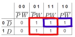
To develop the simplified Boolean equation, look for all the cells with a 1 that can physically be boxed together, where the number of cells in the box is a power of 2 (1, 2, 4, or 8 and so on). The boxes are allowed to overlap so the same cells can be used more than once. Look for the biggest boxes first, and keep finding smaller boxes until all the cells with a 1 in them are used. This means that sometimes just single cells will remain at the end. The cells in the K-map for the ATM example can be grouped as shown in Table 3.
In this example, all the cells containing a 1 were covered with two boxes. This means that if the conditions for either box are 1, the output will be 1. This also means that the simplified Boolean equation will only have two terms. The term for each box can be determined by finding the variables that are constant throughout each cell of that box. For the red box, only W remains constant through the four cells. D switches from the top row to the bottom row, and P switches from the left column to the right column. This means that even though D switches between 0 and 1, and P switches between 0 and 1, the output remains constant. They are irrelevant in determining the output, and only the constant term, W, is relevant for determining the output highlighted by the red box. For the blue box, P and remains constant through the two cells, while W switches from the left cell to the right cell, meaning that is responsible for determining the output of the blue box, and W is irrelevant. The relevant terms for each box are added to produce the simplified Boolean equation shown in (3).
(3)
This equation meets the conditions in the truth table and achieves the desired result with the minimum number of logic elements.
Logic Gates
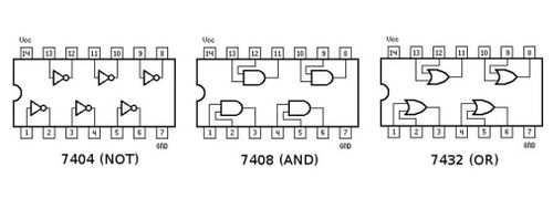
Digital logic is applied to digital circuitry through the use of simple logic gates. There are symbols for each of these gates, and the connections between them are represented by lines running from the output of one gate to the input of another. A line can connect only one output to each input. There are seven gates, but only the NOT, AND and OR gates will be used in this lab (Figure 1).
The NOT gate is an inverter. It has one input and produces its opposite as the output. For example, if a 1 is the input to a NOT gate, a 0 is outputted, as seen in Table 4. The symbol for the operation is a macron or over bar over the variable. The truth table for a NOT gate is shown in Table 4.
| 0 | 1 |
| 1 | 0 |
The AND gate performs a comparison operation on its inputs. If all the inputs are 1, the output is also 1. If either of the inputs is 0, the output is also 0. An AND gate can have two or more inputs (denoted by A and B in Table 5), but two inputs were used in this exercise. The symbol for the AND operation is a dot (·) between the variables , and is represented by multiplication mathematically. The truth table for an AND gate is shown in Table 5.
| 0 | 0 | 0 |
| 0 | 1 | 0 |
| 1 | 0 | 0 |
| 1 | 1 | 1 |
An OR gate performs a comparison operation on its inputs. If either of the inputs is 1, the output is also 1. But if all the inputs are 0, the output is also 0. An OR gate can have two or more inputs, but for this lab, it will have two inputs (denoted by A and B in Table 6). The symbol for the OR operation is a plus (+), and is represented by addition mathematically. The truth table for an OR gate is shown in Table 6.
| 0 | 0 | 0 |
| 0 | 1 | 1 |
| 1 | 0 | 1 |
| 1 | 1 | 1 |
Combinational Logic Circuits
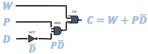
A combinational logic circuit can be created using the simplified equation. A combinational logic circuit is a combination of logic gates that takes in inputs and produces an output according to a truth table or Boolean equation. For the ATM circuit, a NOT operation is performed on by inputting and outputting through a NOT gate. and are inputted into an AND gate, as denoted by them being multiplied in the simplified Boolean equation.The result of the AND operation between the and and the W is inputted into an OR gate, as denoted by the addition function in the Boolean simplified equation. The final combinational logic circuit can be seen in Figure 2.
Integrated Circuits
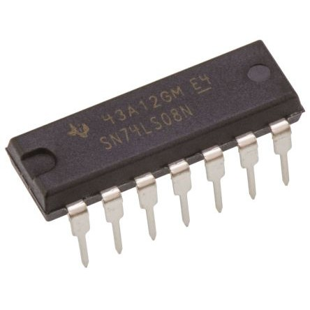
Integrated circuits (IC) can be used to prototype a combinational logic circuit on a breadboard. These devices are small assemblies of electronic components that have been combined into a single unit. In this lab, the IC chips consist of logic gates that can be wired to prototype the logic circuit (Figure 3). For IC chips and other electrical components, power (5V) and ground (0V) represent 1 and 0, respectively.
Each chip consists of multiple logic gates. A 7408 chip consists of four AND gates, a 7432 chip consists of four OR gates, and a 7404 chip consists of six NOT gates. These gates can be wired to inputs and outputs to create a combinational logic circuit. The IC chips must also be connected to a power source and ground to operate.
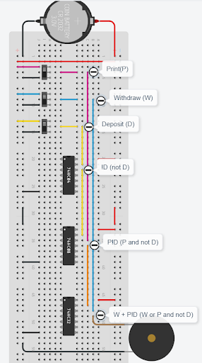
Figure 4 shows how the IC chips can be used to wire the circuit for the ATM problem. In this circuit in Tinkercad, a piezo buzzer represents the output. Slide switches control the Print, Withdraw, and Deposit inputs, where connecting the switch to the power sets the input to 1, and connecting the switch to the ground sets the input to 0. The pink wire represents the Print (P) input, the blue wire represents the Withdraw (W) input, and the yellow wire represents the Deposit (D) inputs.
The input is wired to a NOT gate (IC 7404) to get a output. This output is wired to an AND gate input (IC 7408), along with a input to get a output. This output is wired to an OR gate (IC 7432), along with a W input to get the final output of . In this lab exercise, these steps will be applied to construct the alarm requested by Farmer Georgi.
Basic Breadboard Wiring
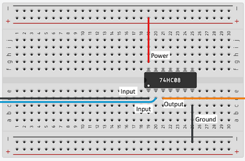
Wire A and Wire B are not connected (Figure 5).
Wire C and Wire D are connected together (Figure 6).
Wire E and Wire F are not connected (Figure 7).
Wire G and Wire H are connected (to be grounded) together. Wire I and Wire J are connected (to be powered) together (Figure 8).
An example of one of the AND gated connected with inputs and outputs for that gate shown (Figure 9). Refer to Figure 1 to see all possible inputs and outputs on an IC chip.
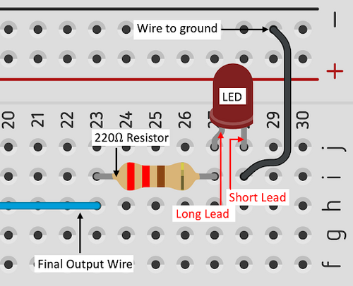
Sample connection for an LED with 220 Ω resistor (Figure 10).
Materials
- 7432 IC (four dual-input OR gates)
- 7408 IC (four dual-input AND gates)
- 7404 IC (six single-input NOT gates)
- Pre-Assembled Breadboard
- Wires
- 5V Battery Case
- LED
- 220 Ω Resistor
- Slide Switches
Procedure
Step 1. Formulate the Simplified Boolean Equation
- The two barns must be assigned a numeric equivalent before the truth table is prepared. Use 1 to represent that a variable (hen, fox, or grain) is in Barn A and 0 to represent that the variable is in Barn B. For the alarm output, use 0 to indicate that the alarm should be off, and 1 to indicate that the alarm should be on. When building the circuit, 1 is power and 0 is ground.
- On a sheet of paper, create a truth table that includes the three inputs (hen, fox, grain) and one output (alarm). Assign the input variables. Use all scenarios for hen, the grain, and the fox. For example, one possible scenario is that the hen, grain and fox are in Barn A, so place a 1 in the three input columns. The number of rows in the truth table should be 2^n where n is the number of inputs.
- Compute the output column. Analyze the three inputs and determine if the alarm will sound for each combination. Place a 1 in the output column if the alarm will sound and a 0 if it will not.
- Circle all the combinations that produce a 1 in the output column. Create the Boolean equation from this table that uses each of the input combinations that produced a 1 output. Refer to the Overview section if there is any confusion.
- Draw a K-map and fill the cells in using the truth table as discussed in the Overview.
- Box the groups of 1s. The 1s may only be boxed in powers of 2. Start with the largest box, and continue to the smallest, making sure to box each cell containing a 1, and also making sure to have as few boxes as possible. Once all the boxes are drawn, identify the constant variables for each box to create the simplified Boolean equation.
- Draw a combinational logic circuit of the simplified Boolean equation. Use a light bulb to represent the alarm. EG1004 recommends using logic.ly for creating the combinational logic circuit. Screenshot the circuit instead of saving it.
- Have a TA approve the combinational logic circuit.
Step 2. Test the Integrated Circuits (ICs)
This step will be done by the lab TAs. Read the following explanation for Step 2 and let the lab TAs know when the ICs are ready to test.
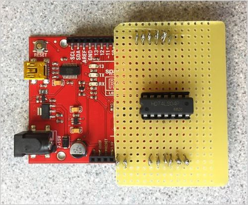
Before building the circuit, the ICs used in wiring the alarm system must be tested to determine if they are functioning. If the procedure is completed without verifying that the ICs work, it will require additional time and troubleshooting when the alarm circuit is built. The system for checking the ICs uses an Arduino board to send and receive signals from the AND/OR/NOT chips and determines if they are functioning properly.
Load the chip onto the Arduino board (Figure 11) and start the Serial Monitor on the Arduino program (top right corner). The code will cycle through the basic inputs (0, 1 for NOT; 00, 01, 10, 11 for AND/OR) and then send the outputs of each gate in the chip back to the Arduino board. The code compares those results to the expected result. It displays each input/output pair and the final result. After the test is done, carefully remove the chips from the test station.
Step 3. Build the Combinational Logic Circuit
- Obtain a pre-assembled breadboard from the TA.
- Build the circuit on a pre-assembled breadboard. On the board, identify each of the three IC chips as an AND, OR, or NOT gate. To do this, read the number on the chip and match it with the numbers shown in Figure 12. Look for the notch at one end of each chip to orient the chip to the diagrams in Figure 12 and to match the pins. Note that each IC chip has multiple gates.
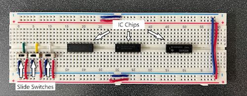
- Place the IC chips over the bridge in the breadboard with the NOT chip on top, the AND chip in the middle, and the OR chip at the end (Figure 13). Remember to orient the IC chips using the notch.
- Power the chips by inserting one end of an electrical lead into the power column marked + on the breadboard. Insert the other end of the lead into Pin 14 of the IC chip. Refer to Figure 7 for the pin numbers on each IC chip. Repeat this process for all three chips.
- Ground the chips by inserting one end of another electrical lead into the ground column marked – on the breadboard and the other end into Pin 7 of the IC chip. Repeat this process for all three chips (Figure 14).
- Using three switches on the breadboard, assign each switch to an input variable (fox, grain, hen). For all three switches, the wire connected to the ground represents Barn A, and the wire connected to power represents Barn B.
- The center leads from each switch begins the wiring for each input variable. Follow Figure 12 to connect to the inputs and outputs of each gate on the IC chip.
- Continue this process until the entire circuit is wired according to the simplified Boolean equation. Insert one end of a wire into the final output of the logic circuit (This will most likely be the output of an OR gate). Attach the other end of the wire to the last row of the breadboard where no other connections are made. This will serve as the connection for the power side of the LED. The LED must also be grounded. Ensure that a 220 Ω resistor is added connecting the negative terminal of the LED and ground.
- Have a TA verify and approve the wiring before supplying any power to the circuit.
- Ensure the 5 V Battery is powered off. Wire the positive (red) wire to the power line of the breadboard. Repeat this process for the ground (black) wire, and wire it to the ground power line of the breadboard. These wires will serve as the power and ground for all the IC chips and the slide switches. Power the battery and observe the LED.
- Operate the slide switches corresponding to the fox, grain, and hen. Observe the LED to see if the alarm goes off based on the inputs to each barn. Compare the results to the truth table to determine if the circuit is operating correctly.
- If the circuit is not operating properly, disconnect the circuit from power and examine the circuit including the wiring.
- If the circuit is operating correctly, take pictures of the circuit and clean up the workspace.
The lab work is now complete. Refer to the Assignment section for the instructions to prepare the lab report.
Assignment
Individual Lab Report
Follow the lab report guidelines laid out in the EG1004 Writing Style Guide in the Technical Writing section of the manual. Use the outline below to write this report.
- Abstract
- Briefly state the objective of the lab, note that the circuit was tested, and summarize its behavior when it was tested
- Introduction
- Define and discuss digital logic
- Define and discuss the use of truth tables, Boolean equations, K Maps, and simplified Boolean equations in designing and building digital circuits. Use the ATM problem to illustrate their use in designing and building digital circuits
- Define and discuss logic gates generally, describe the behavior of the three logic gates used in this lab, and note that they implement digital logic in digital circuitry
- Discuss integrated circuits
- Briefly describe the problem statement for this lab
- Procedure
- In a sentence, present the materials used in this lab
- Describe the steps taken to complete the lab, including a description of how the circuit was tested at the end of this section. Do NOT include the test results in this section. Use incomplete versions of the truth table and K map to show how they were created. Do NOT include completed versions of the truth table and K map in this section. Describe the Boolean equations (i.e. “The original Boolean equation used six three-variable terms…”), but do NOT include them in this section
- Data/Observations
- In paragraphs, present and discuss the completed truth table, the original Boolean equation, the K map, and the simplified Boolean equation in this section. Summarize the test results in this section and note the results were compared to the output in the truth table to determine if the circuit operated correctly
- Conclusion
- Discuss the value of the minimization that results from the use of a K map. Compare how many gates would be used if the original Boolean equation was used to build the alarm circuit versus the number of gates used to build the alarm circuit using the simplified Boolean equation
- Discuss how minimization, digital logic, and combinational logic circuits have advanced technology
- Discuss any improvements
Remember: Lab notes must be taken. Experimental details are easily forgotten unless written down. EG1004 Lab Notes paper can be downloaded and printed from the EG1004 Website. Use the lab notes to write the Procedure section of the lab report. At the end of each lab, a TA will scan the lab notes and upload them to the Lab Documents section of the EG1004 Website. One point of extra credit is awarded if the lab notes are attached at the end of the lab report. Keeping careful notes is an essential component of all scientific practice.
Team Powerpoint Presentation
Follow the presentation guidelines laid out in the EG1004 Lab Presentation Format in the Technical Presentations section of the manual. When preparing the presentation, consider the following points.
- How does digital logic impact the world today?
- What considerations should be made to prototype a circuit?
- Include the truth table, Boolean equation, K-map, simplified Boolean equation, and combinational logic circuit developed during the lab
References
| ||||||||


 and
and  , respectively. On the truth table with the inputs PDW = 000, the output is 0, and that is used to fill the cell. This is repeated for every cell in the K-map. Table 2 is the K-map for the ATM example.


 is responsible for determining the output of the blue box, and W is irrelevant. The relevant terms for each box are added to produce the simplified Boolean equation shown in (3).



 output. This output is wired to an AND gate input (IC 7408), along with a
  output. This output is wired to an OR gate (IC 7432), along with a W input to get the final output of
  .
In this lab exercise, these steps will be applied to construct the alarm requested by Farmer Georgi.
