Difference between revisions of "Electronic Filters"
m |
|||
| (One intermediate revision by the same user not shown) | |||
| Line 5: | Line 5: | ||
<p>The experimental objective of this lab is to build three | <p>The experimental objective of this lab is to build three | ||
electrical circuits and to test them using a virtual bench oscilloscope in | electrical circuits and to test them using a virtual bench oscilloscope in | ||
order to identify each as a low-, high-, or band-pass filter. The -<b><i>3dB point </i></b>for each filter will also be identified.</p> | order to identify each as a low-, high-, or band-pass filter. The -<b><i>3dB point | ||
</i></b>for each filter will also be identified.</p> | |||
<p>Together, we will learn how <b><i>electrical | <p>Together, we will learn how <b><i>electrical | ||
| Line 75: | Line 76: | ||
varying frequencies is shown in Figure 9.1.</p> | varying frequencies is shown in Figure 9.1.</p> | ||
<p align=center>[[image: | <p align=center>[[image:lab_filters_1.gif]]</p> | ||
<p class=caption>Figure 9.1: Capacitor frequency response</p> | <p class=caption>Figure 9.1: Capacitor frequency response</p> | ||
| Line 91: | Line 92: | ||
across an inductor and varying frequencies is shown in Figure 9.2.</p> | across an inductor and varying frequencies is shown in Figure 9.2.</p> | ||
<p align=center>[[image: | <p align=center>[[image:lab_filters_2.gif]]</p> | ||
<p class=caption>Figure 9.2: Inductor frequency response</p> | <p class=caption>Figure 9.2: Inductor frequency response</p> | ||
| Line 110: | Line 111: | ||
9.3.</p> | 9.3.</p> | ||
<p align=center>[[image: | <p align=center>[[image:lab_filters_4.gif]]</p> | ||
<p class=caption>Figure 9.3: Component schematic symbols</p> | <p class=caption>Figure 9.3: Component schematic symbols</p> | ||
| Line 123: | Line 124: | ||
V<sub>A</sub> + V<sub>B</sub> + V<sub>C</sub></i>).</p> | V<sub>A</sub> + V<sub>B</sub> + V<sub>C</sub></i>).</p> | ||
<p align=center>[[image: | <p align=center>[[image:lab_filters_5.jpg]]</p> | ||
<p class=caption>Figure 9.4: A serial circuit</p> | <p class=caption>Figure 9.4: A serial circuit</p> | ||
| Line 132: | Line 133: | ||
the same (<i>V<sub>IN</sub> = V<sub>D</sub> = V<sub>E</sub></i>)).</p> | the same (<i>V<sub>IN</sub> = V<sub>D</sub> = V<sub>E</sub></i>)).</p> | ||
<p align=center>[[image: | <p align=center>[[image:lab_filters_6.jpg]]</p> | ||
<p class=caption>Figure 9.5: A parallel circuit</p> | <p class=caption>Figure 9.5: A parallel circuit</p> | ||
| Line 138: | Line 139: | ||
<p>Serial and parallel circuits can be combined, as shown in Figure 9.6:</p> | <p>Serial and parallel circuits can be combined, as shown in Figure 9.6:</p> | ||
<p align=center>[[image: | <p align=center>[[image:lab_filters_25.jpg]]</p> | ||
<p class=caption>Figure 9.6: A hybrid circuit</p> | <p class=caption>Figure 9.6: A hybrid circuit</p> | ||
| Line 188: | Line 189: | ||
why the cutoff frequency is important.</p> | why the cutoff frequency is important.</p> | ||
<p align=center>[[image: | <p align=center>[[image:lab_filters_8.gif]]</p> | ||
<p class=caption>Figure 9.7: Characteristic behavior of a low-pass filter</p> | <p class=caption>Figure 9.7: Characteristic behavior of a low-pass filter</p> | ||
| Line 201: | Line 202: | ||
frequency.</p> | frequency.</p> | ||
<p align=center>[[image: | <p align=center>[[image:lab_filters_11.gif]]</p> | ||
<p class=caption>Figure 9.8: Characteristic behavior of a high-pass filter</p> | <p class=caption>Figure 9.8: Characteristic behavior of a high-pass filter</p> | ||
| Line 214: | Line 215: | ||
band-pass filter.</p> | band-pass filter.</p> | ||
<p align=center>[[image: | <p align=center>[[image:lab_filters_12.gif]]</p> | ||
<p class=caption>Figure 9.9: Characteristic behavior of a band-pass filter</p> | <p class=caption>Figure 9.9: Characteristic behavior of a band-pass filter</p> | ||
| Line 228: | Line 229: | ||
that the first two rows and the last two rows are connected <b><i>horizontally</i></b>; the other rows are connected <b><i>vertically</i></b>, as shown in Figure 9.10.</p> | that the first two rows and the last two rows are connected <b><i>horizontally</i></b>; the other rows are connected <b><i>vertically</i></b>, as shown in Figure 9.10.</p> | ||
<p align=center>[[image: | <p align=center>[[image:lab_filters_14.gif]]</p> | ||
<p class=caption>Figure 9.10: Breadboard layout</p> | <p class=caption>Figure 9.10: Breadboard layout</p> | ||
| Line 239: | Line 240: | ||
how many zeroes to add. Each colored band represents a particular number.</p> | how many zeroes to add. Each colored band represents a particular number.</p> | ||
<p align=center>[[image: | <p align=center>[[image:lab_filters_16.gif]]</p> | ||
<p class=caption>Figure 9.11: Color-coded bands on a 1KΩ resistor</p> | <p class=caption>Figure 9.11: Color-coded bands on a 1KΩ resistor</p> | ||
| Line 537: | Line 538: | ||
<li>The DAC board has two wires attached to pins <b><i>3 </i></b>and <b><i>4</i></b>. Connect | <li>The DAC board has two wires attached to pins <b><i>3 </i></b>and <b><i>4</i></b>. Connect | ||
the <b><i><font color=#ff0000>red</font></i></b> alligator clip of the connecting cable to the other | the <b><i><font color=#ff0000>red</font></i></b> alligator clip of the connecting cable to the other | ||
end of the pin 3<b><i> </i></b>wire and connect the <b><i>black </i></b>alligator clip of the connecting cable to the other | end of the pin 3<b><i> </i></b>wire and connect the <b><i>black </i></b>alligator clip of | ||
end of the pin <b><i>4 </i></b>wire.</li> | the connecting cable to the other end of the pin <b><i>4 </i></b>wire.</li> | ||
<li>Turn on the function generator using the green button. | <li>Turn on the function generator using the green button. | ||
| Line 548: | Line 549: | ||
until the display reads <b><i>1.000KHz</i></b>.</li> | until the display reads <b><i>1.000KHz</i></b>.</li> | ||
<li>On your lab PC, with the Virtual | <li>On your lab PC, with the Virtual Bench Oscilloscope open, click Auto Setup. It will look | ||
Bench | like Figure 9.12.</li> | ||
<li>On the function | <li>On the function | ||
| Line 559: | Line 560: | ||
Setup�? again.</li> | Setup�? again.</li> | ||
<p align=center><b>[[image: | <p align=center><b>[[image:lab_filters_17.jpg]]</b></p> | ||
<p class=caption>Figure 9.12: The Virtual Bench | <p class=caption>Figure 9.12: The Virtual Bench Oscilloscope program window</p> | ||
<li>When you have finished calibrating the function | <li>When you have finished calibrating the function | ||
generator and the Virtual Bench | generator and the Virtual Bench Oscilloscope software, the <b><i>Volts peak to peak (Vp-p) </i></b>reading | ||
on your lab PC will be approximately 2.00V. Record the <i>Vp</i><i>-p </i>reading. This is your <i>V<sub>IN</sub></i>. Use | on your lab PC will be approximately 2.00V. Record the <i>Vp</i><i>-p </i>reading. This is your <i>V<sub>IN</sub></i>. Use | ||
this figure for all your computations. Also, calculate .707*V<sub>IN</sub> and | this figure for all your computations. Also, calculate .707*V<sub>IN</sub> and | ||
| Line 574: | Line 575: | ||
</i>Duty <i>knobs for first two circuits. If you do, | </i>Duty <i>knobs for first two circuits. If you do, | ||
you will have to recalibrate both the function generator and the </i>Virtual | you will have to recalibrate both the function generator and the </i>Virtual | ||
Bench | Bench Oscilloscope<i>.</i></p> | ||
<li>Now we will build <b><i>Circuit 1</i></b>. Shut off | <li>Now we will build <b><i>Circuit 1</i></b>. Shut off | ||
| Line 580: | Line 581: | ||
Use the schematic diagram in Figure 9.13 to build your circuit.</li> | Use the schematic diagram in Figure 9.13 to build your circuit.</li> | ||
<p align=center>[[image: | <p align=center>[[image:lab_filters_20.gif]]</p> | ||
<p class=caption>Figure 9.13: Circuit 1 (R = 100KΩ, C = 0.0001µF)</p> | <p class=caption>Figure 9.13: Circuit 1 (R = 100KΩ, C = 0.0001µF)</p> | ||
| Line 595: | Line 596: | ||
<li>Now you | <li>Now you | ||
will insert two wires into the breadboard to connect your circuit to the Virtual | will insert two wires into the breadboard to connect your circuit to the Virtual | ||
Bench | Bench Oscilloscope software (via the DAC board). To do this, connect the wire of pin <b><i>3</i></b> | ||
that your resistor and capacitor share. Insert the wire coming from pin <b><i>4 </i></b>of the DAC board into the breadboard in the same | of your DAC board to the breadboard in the same column that your resistor and capacitor share. | ||
Insert the wire coming from pin <b><i>4 </i></b>of the DAC board into the breadboard in the same | |||
column as the spare lead of your capacitor.</li> | column as the spare lead of your capacitor.</li> | ||
| Line 604: | Line 606: | ||
i.e. the one not connected to the resistor, and that also has one of the wires | i.e. the one not connected to the resistor, and that also has one of the wires | ||
connected to it from the DAC board. If you have wired your circuit | connected to it from the DAC board. If you have wired your circuit | ||
successfully, the Virtual Bench | successfully, the Virtual Bench Oscilloscope software will have a | ||
horizontal line across the center of the screen.</li> | horizontal line across the center of the screen.</li> | ||
<li>Turn on | <li>Turn on the function generator. Change the frequency on the function generator in this | ||
the function generator. Change the frequency on the function generator in this | pattern (10, 20, 50, 100, 200, 500, 1000, 2000, 5000, 10000Hz) and record the <i>Vp</i><i>-p</i> | ||
pattern (10, 20, 50, 100, 200, 500, 1000, 2000, 5000, 10000Hz) and record the <i>Vp</i><i>-p </i>reading at each frequency for a | reading at each frequency for a total of 10 measurements. Looking at your results, you will see | ||
total of 10 measurements. Looking at your results, you will see voltages above | voltages above and below the -3dB point voltage. Now find the- 3dB point exactly by starting | ||
and below the -3dB point voltage. Now find the- 3dB point exactly by starting | |||
with the frequency just below the -3dB point, and then increasing the frequency | with the frequency just below the -3dB point, and then increasing the frequency | ||
until you have the voltage corresponding to the -3dB point. Note the frequency | until you have the voltage corresponding to the -3dB point. Note the frequency | ||
| Line 620: | Line 621: | ||
build <b><i>Circuit 2</i></b>.</li> | build <b><i>Circuit 2</i></b>.</li> | ||
<p align=center>[[image: | <p align=center>[[image:lab_filters_22.gif]]</p> | ||
<p class=caption>Figure 9.14: Circuit 2 (R = 1 MΩ, C = 0.001µF).</p> | <p class=caption>Figure 9.14: Circuit 2 (R = 1 MΩ, C = 0.001µF).</p> | ||
| Line 626: | Line 627: | ||
<li>Insert | <li>Insert | ||
two wires into the breadboard to connect your circuit to the Virtual | two wires into the breadboard to connect your circuit to the Virtual | ||
Bench | Bench Oscilloscope software (via the DAC board). Connect the wire of pin <b><i>3 </i></b>of your | ||
that your resistor and capacitor share. Insert the wire coming from pin <b><i>4 </i></b>of the DAC board into the breadboard in the same | DAC board to the breadboard in the same column that your resistor and capacitor share. Insert the | ||
wire coming from pin <b><i>4 </i></b>of the DAC board into the breadboard in the same | |||
column as the spare lead of your resistor.</li> | column as the spare lead of your resistor.</li> | ||
<li>Connect the <b><i><font color=#ff0000>red</font></i></b> alligator clip from the function generator to left end | <li>Connect the <b><i><font color=#ff0000>red</font></i></b> alligator clip from the function | ||
of the resistor, i.e. the one not connected to the capacitor. Connect the <b><i>black </i></b>alligator clip to the bottom lead of the capacitor, | generator to left end of the resistor, i.e. the one not connected to the capacitor. Connect the | ||
i.e. the one not connected to the resistor, and that also has one of the wires | <b><i>black</i></b> alligator clip to the bottom lead of the capacitor, i.e. the one not connected | ||
connected to it from the DAC board. If you have wired your circuit | to the resistor, and that also has one of the wires connected to it from the DAC board. If you have | ||
successfully, the Virtual Bench | wired your circuit successfully, the Virtual Bench Oscilloscope software will have a horizontal line | ||
horizontal line across the center of the screen.</li> | across the center of the screen.</li> | ||
<li>Turn on | <li>Turn on the function generator. Change the frequency on the function generator in this | ||
the function generator. Change the frequency on the function generator in this | pattern (10, 20, 50, 100, 200, 500, 1000, 2000, 5000, 10000Hz) and record the <i>Vp</i><i>-p</i> | ||
pattern (10, 20, 50, 100, 200, 500, 1000, 2000, 5000, 10000Hz) and record the <i>Vp</i><i>-p </i>reading at each frequency for a | reading at each frequency for a total of 10 measurements. Looking at your results, you will see | ||
total of 10 measurements. Looking at your results, you will see voltages above | voltages above and below the -3dB point voltage. Now find the -3dB point exactly by starting | ||
and below the -3dB point voltage. Now find the -3dB point exactly by starting | |||
with the frequency just below the -3dB point, and then increasing the frequency | with the frequency just below the -3dB point, and then increasing the frequency | ||
until you have the voltage corresponding to the -3dB point. Note the frequency | until you have the voltage corresponding to the -3dB point. Note the frequency | ||
and write it down. This is the cutoff frequency.</li> | and write it down. This is the cutoff frequency.</li> | ||
<li>Shut off | <li>Shut off the function generator and disconnect the all the wires, capacitors, and | ||
the function generator and disconnect the all the wires, capacitors, and | |||
resistors from the breadboard. Use the schematic diagram in Figure 9.15 to | resistors from the breadboard. Use the schematic diagram in Figure 9.15 to | ||
build <b><i>Circuit 3</i></b>. Note that the circuit is symmetrical, and that both the input and | build <b><i>Circuit 3</i></b>. Note that the circuit is symmetrical, and that both the input and output | ||
of the circuit are connected to the two ends of the inductor and capacitor.</li> | of the circuit are connected to the two ends of the inductor and capacitor.</li> | ||
<p align=center>[[image: | <p align=center>[[image:lab_filters_24.gif]]</p> | ||
<p class=caption>Figure 9.15: Circuit 3 (C = 100µF, L = 1mH)</p> | <p class=caption>Figure 9.15: Circuit 3 (C = 100µF, L = 1mH)</p> | ||
<li>Insert two wires into the breadboard to connect your circuit to the Virtual | <li>Insert two wires into the breadboard to connect your circuit to the Virtual Bench Oscilloscope | ||
software (via the DAC board). Connect the wire of pin <b><i>3 </i></b>of your DAC board to the | |||
that your inductor and capacitor share. Insert the wire coming from pin <b><i>4 </i></b>of the DAC board into the breadboard in the other | breadboard in one of columns that your inductor and capacitor share. Insert the wire coming from pin | ||
column shared by the inductor and capacitor.</li> | <b><i>4</i></b> of the DAC board into the breadboard in the other column shared by the inductor and | ||
capacitor.</li> | |||
<li>Connect the <b><i><font color=#ff0000>red</font></i></b> alligator clip from the function generator to the top lead of the capacitor. | <li>Connect the <b><i><font color=#ff0000>red</font></i></b> alligator clip from the function generator | ||
Connect the <b><i>black </i></b>alligator clip to the bottom lead of the capacitor. If you have wired your circuit | to the top lead of the capacitor. Connect the <b><i>black </i></b>alligator clip to the bottom lead of the | ||
successfully, the Virtual | capacitor. If you have wired your circuit successfully, the Virtual Oscilloscope software will have a | ||
horizontal line across the center of the screen.</li> | horizontal line across the center of the screen.</li> | ||
<p><i><b>Note:</b> At this point you will be changing the voltage on the signal generator for the first time since the start of the lab. | <p><i><b>Note:</b> At this point you will be changing the voltage on the signal generator for the first | ||
However, once you have changed the voltage with the next step, do not change the voltage again for the rest of the lab or you will have | time since the start of the lab. However, once you have changed the voltage with the next step, do not | ||
to restart from the next step forward.</i></p><br> | change the voltage again for the rest of the lab or you will have to restart from the next step | ||
forward.</i></p><br> | |||
<li>Turn on the function generator. This circuit | <li>Turn on the function generator. This circuit | ||
| Line 695: | Line 697: | ||
the cutoff frequency.</li> | the cutoff frequency.</li> | ||
<li>Shut off the function generator and disconnect the all the wires, capacitors, and resistors from the breadboard. You have now completed the lab.</li> | <li>Shut off the function generator and disconnect the all the wires, capacitors, and | ||
resistors from the breadboard. You have now completed the lab.</li> | |||
Revision as of 18:12, 13 July 2005
EG1004 Lab 9: Electronic Filters
9.1 OBJECTIVES
The experimental objective of this lab is to build three electrical circuits and to test them using a virtual bench oscilloscope in order to identify each as a low-, high-, or band-pass filter. The -3dB point for each filter will also be identified.
Together, we will learn how electrical filters are used, how resistors, capacitors, and inductors function in a filter and the significance of the -3dB point.
9.2 OVERVIEW
It is important for electrical engineers to be able to selectively filter certain frequencies. An electrical filter works by allowing only designated frequencies to pass through. By tuning your radio to a particular station, you are isolating a certain frequency. The filter selects the station you have chosen from the hundreds of different stations that are broadcasting. How does the filter accomplish this?
To understand how filters work, we need to identify the elements that make electrical filtering possible. Signals that occur naturally are composed of many frequencies.
For example, the human voice is composed of frequencies ranging from 0–4KHz. A signal consists of a primary frequency, called a base frequency, plus additional multiples of that frequency with different loudness called harmonics. Different devices will have different harmonics. This is why when a trumpet and clarinet both play the same musical note they sound different — their harmonics are different. We hear the base frequency plus the harmonics of these instruments. Radio waves work differently than sound waves. The signal has a base frequency, and the information we hear is contained in adjacent frequencies called sidebands.
Voltage, or electromotive force, and frequency are the building blocks of an electrical signal. Voltage is a force that propels electrons through a medium. Current is the amount of electric charge flowing past a specified circuit point per unit time. Frequency is the rate at which the signal repeats itself. The gain of a circuit is the ratio of its power compared to its input. For devices that do not produce energy, such as this lab, the gain cannot exceed one. However for devices such as transistors and other amplifiers, the gain can be much greater than one.
A filter is a circuit that shapes and controls the bandwidth of a signal; bandwidth is the range of frequencies that the filter allows to pass. For example, when we turn up the bass of an audio amplifier, we are using a filter that passes the low frequencies more than the high frequencies. Also, when we tune a radio, we are using a filter that allows the base frequency plus the sidebands of the desired station to pass, but not other stations.
The filters that we are going to build are composed of resistors, capacitors, and inductors. A resistor resists the flow of electrons by converting some of the electric energy to heat. The voltage across a resistor obeys Ohm's Law: V = IR, where I is the current and R is the resistance. Varying the frequency of the voltage will not affect the voltage across the resistor.
A resistor is designed to impede the flow of electricity and dissipate electrical energy in the form of heat. Resistors work by having the electricity flow through a poor conductor such as carbon. The unit of resistance is the Ohm, named after Georg Ohm, and is represented by the capital Greek letter Omega (“Ω�?).
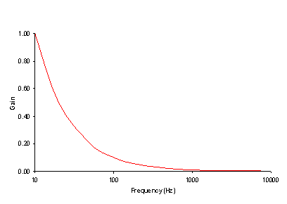
Capacitors are metal plates that are separated from each other, allowing electric charge to accumulate on the plates. These plates store energy rather than dissipate it, like a resistor. For DC voltage, provided by a device like a battery, the plates will gather charge, and once the plates are charged, will no longer pass current, so the capacitor looks like an “open circuit�?, where nothing is connected. For high frequencies, the charge can quickly gather and dissipate off the plates, allowing current to flow through the capacitor freely, making the capacitor behave like a “short circuit�?. The unit of capacitance is the Farad, named after Michael Faraday, and is represented by the capital letter “F�?. The relationship between the voltage across a capacitor and varying frequencies is shown in Figure 9.1.
Figure 9.1: Capacitor frequency response
Inductors, also known as coils or chokes, are coils of wire that allow the current through the wire to form a magnetic field. Like capacitors, inductors store energy, but in the magnetic field instead of on plates, and its behavior is the opposite of a capacitor. For DC voltage, the current will make a stable magnetic field and the current will flow freely, making the inductor look like a “short circuit�?. At high frequencies, the magnetic field does not have time to form before the current reverses and the field collapses, causing the inductor to resist the current flow, looking like an “open circuit�?. The unit of inductance is the Henry, named after Joseph Henry, and is represented by the capital letter “H�?. The relationship between the voltage across an inductor and varying frequencies is shown in Figure 9.2.
Figure 9.2: Inductor frequency response
The elements of filters, such as resistors, capacitors, and inductors, are connected by conductors (wires) that carry electrons between these devices. The voltage is the same throughout the entire conductor, so the voltage across the two ends of the conductor is zero.
How the components are connected is shown using a schematic diagram. Each component is represented by a symbol, and the connections between components are represented by lines. The symbols are designed to represent the physical characteristics of the components. Therefore, a resistor is represented by a zigzag line showing how the electricity’s path is impaired. A capacitor is shown as two parallel lines, representing its plates. Finally, an inductor is shown as a series of looping lines, representing the coils of wire it has. The schematic diagram symbols for these components are shown in Figure 9.3.
Figure 9.3: Component schematic symbols
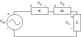
Different combinations of resistors and capacitors allow engineers to build different kinds of filters to perform specific tasks. Resistors, inductors, and capacitors can be arranged in three different ways. In a series circuit, the element's conductors are connected end to end. The current in a series circuit remains the same in all the electrical elements. In a serial circuit, as shown in Figure 9.4, the sum of the voltages across each element is equal to the voltage of the power source (VIN = VA + VB + VC).
Figure 9.4: A serial circuit
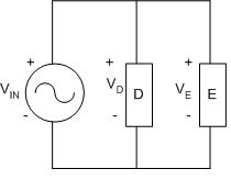
In a parallel circuit, as shown in Figure 9.5, the element's conductors are connected at opposing ends. The current that is supplied by the voltage source equals the current that flows though elements D, E, and F. The voltage across the elements that are parallel is the same (VIN = VD = VE)).
Figure 9.5: A parallel circuit
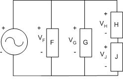
Serial and parallel circuits can be combined, as shown in Figure 9.6:
Figure 9.6: A hybrid circuit
The voltage across the cop and bottom connectors is the same, so (VIN = VF = VG = (VG + VJ)).
To produce a graphical representation of the characteristic behavior of the circuit being analyzed, it is necessary to graph the gain of the circuit versus the frequency of the electrical signal. Gain is a measure of the power produced by the circuit, measured in decibels, and is calculated using the following formula:
A 3dB drop of signal power from the highest point on the gain vs. frequency graph is the point at which the signal power is half of its original value. The frequency corresponding to this -3dB point is also called the cutoff frequency of the filter. Note that since the filters we are using only contain passive components, the output cannot be larger than the input. Therefore, the gain will always be a negative number because we are taking the logarithm of a number less than one.
If you examine the preceding formula, you’ll see that for the gain to be -3dB, VOUT must be VIN divided by the square root of 2, more easily written as VOUT=.707*VIN. Therefore, the -3dB point of a circuit is the frequency that causes the output voltage to be .707 times the input voltage.
Types of Filters
Your job, once you have built the electrical filters according to the specifications in this manual, is to identify them. In order to do this, we must define the three possibilities.
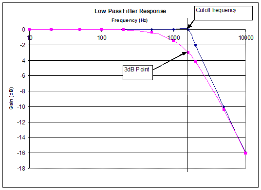
Sometimes, it is beneficial to remove the high frequency components from a signal because this is where unwanted noise frequently exists. To do this, a low-pass filter is used. It passes the low frequencies while blocking the higher ones. The low-pass filter shown here has a gain that drops from 0dB to -3dB at 1590 Hz, which is its -3dB point and corresponding cut-off frequency. Thus, the filter has a bandwidth of 1590Hz and it only allows frequencies from 0Hz to 1590Hz to pass through at full power. Figure 9.7 shows the characteristic behavior of a low-pass filter. A trend line showing the response of the filter is also shown. Note that for low frequencies, the gain is 0dB, meaning that the output equals the input. The filter suppresses high frequencies, as shown by the trend line on the right. The intersection of these two trend lines will be at the cutoff frequency, giving another reason why the cutoff frequency is important.
Figure 9.7: Characteristic behavior of a low-pass filter
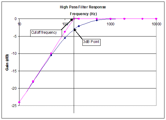
A high-pass filter passes the high frequencies but blocks the low ones, the opposite response of a low-pass filter. The -3dB point for this filter is 160 Hz. This is determined using the same method we used for the low-pass filter. Thus, we can say that the filter has a bandwidth of 60 Hz to infinity and that the filter only allows frequencies greater than 160 Hz to pass through. Figure 9.8 shows the characteristic behavior of a high-pass filter as well as the trend lines and their intersection at the cutoff frequency.
Figure 9.8: Characteristic behavior of a high-pass filter
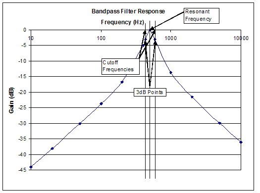
A band-pass filter only allows a certain range of frequencies to pass through and blocks all other frequencies. The frequency of the highest response point is called the resonant frequency, and is defined to be 0dB. This type of filter has two -3dB points, one above the resonant frequency and one below it, and therefore two cutoff frequencies. The difference in these two cutoff frequencies is called the bandwidth of the band-pass filter. Figure 9.9 shows the characteristic behavior of a band-pass filter.
Figure 9.9: Characteristic behavior of a band-pass filter
The band-pass filter shown here has a resonant frequency of approximately 500Hz, and has -3dB points with cutoff frequencies of approximately 400Hz and 600Hz. Therefore, the bandwidth of this filter is approximately 600Hz-400Hz, or 200Hx.
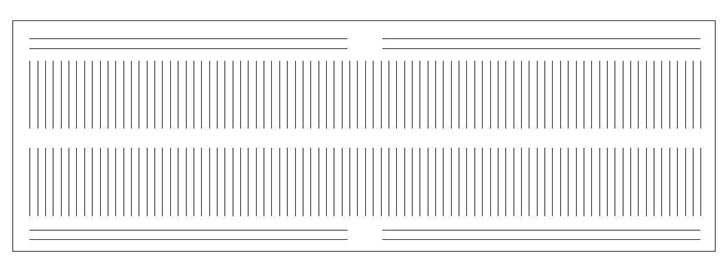
Now, we are ready to build the circuits that will produce the three electrical filters. Before we start, it is important to understand the breadboard we will be using to connect the elements of our circuits. Remember that the first two rows and the last two rows are connected horizontally; the other rows are connected vertically, as shown in Figure 9.10.
Figure 9.10: Breadboard layout
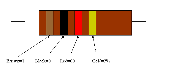
Finally, you'll need to identify the resistors and the capacitors required to complete your circuit. To identify the resistors, you must look at the colored bands. Hold the resistor horizontally with the three bands that are close together to the left, as shown in Figure 9.11. The first two colors determine the first two digits of the resistance, and the third band determines how many zeroes to add. Each colored band represents a particular number.
Figure 9.11: Color-coded bands on a 1KΩ resistor
Resistor color code:
|
Color |
First Band |
Second Band |
Third Band |
|
Black |
0 |
0 |
X1 |
|
Brown |
1 |
1 |
X10 |
|
Red |
2 |
2 |
X100 |
|
Orange |
3 |
3 |
X1000 |
|
Yellow |
4 |
4 |
X10000 |
|
Green |
5 |
5 |
X100000 |
|
Blue |
6 |
6 |
X106 |
|
Violet |
7 |
7 |
X107 |
|
Gray |
8 |
8 |
X108 |
|
White |
9 |
9 |
X109 |
The fourth band indicates a tolerance of the resistor, which means how close its actual resistance will be to the value indicated by the bands:
|
Color |
Tolerance |
|
Gold |
5% |
|
Silver |
10% |
|
No band |
20% |
As an example, a 470KΩ resistor with a 5% tolerance would have color bands of yellow, violet, yellow, and gold. You should check this yourself to be sure you know how to read the colors.
For capacitors, the value is stamped on the capacitor. Sometimes the value is coded. If you can’t read the capacitor value, ask your TA for help.
For inductors, the value is stamped on the inductor. If you can’t find the value, ask your TA for help.
9.3 YOUR ASSIGNMENT
Team PowerPoint Presentation and Individual Lab Report
(one report per student)
The following discussion points are to be addressed in the appropriate section of both your lab report and presentation:
- What is an oscilloscope? You may have to do some research to answer this question.
- Observe the graphs generated from each circuit. What type of filter does each circuit produce?
- Does each circuit produce the expected result? If not, explain why.
- Locate the -3dB point on each graph and cutoff frequency to determine the bandwidth of each filter.
- What is the -3dB point used for?
- Name 3 objects that use filters.
- - Discuss any problems encountered.
9.4 MATERIALS AND EQUIPMENT
- 100KΩ Resistor
- 1MΩ Resistor
- 0.001µF Capacitor
- 0.01µF Capacitor
- 100µF Capacitor
- 1mH Inductor
- Function Generator with Cable
- Breadboard
- DAC Board
- Appropriate Wiring
9.5 PROCEDURE
Circuit Testing
Remember: You are required to take notes. Experimental details are easily forgotten unless written down. You should keep a laboratory notebook for this purpose. Use your lab notes to write the Procedure section of your lab report. You must attach a copy of your lab notes to the WC copy of your lab report. Keeping careful notes is an essential component of all scientific practice.
- Click “Start�?, then �?Lab Menu�?, and select “Lab 9�? off the pull down menu. From there, select “Virtual Bench�?. This will open the Virtual Bench window. Select the first icon, which is “Virtual Bench Scope�?. Make the oscilloscope full screen so that it’s easy to read.
- Plug in the function generator and turn it on.
- Connect the function generator to the DAC board. Each lab PC has a DAC board connected to it by a ribbon cable. Make sure your green DAC board is connected to the analog ribbon cable. Insert the coaxial end of the connecting cable into the 50Ω output on the function generator.
- The DAC board has two wires attached to pins 3 and 4. Connect the red alligator clip of the connecting cable to the other end of the pin 3 wire and connect the black alligator clip of the connecting cable to the other end of the pin 4 wire.
- Turn on the function generator using the green button. Set the range on the function generator to 1KHz. Set the function mode to Sine Wave (~ - the rightmost button of the group of three on the right top side of the function generator). Tune the output frequency to exactly 1KHz by adjusting first the Coarse and then the Fine knobs until the display reads 1.000KHz.
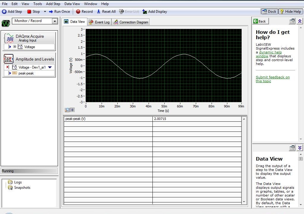
- On your lab PC, with the Virtual Bench Oscilloscope open, click Auto Setup. It will look like Figure 9.12.
- On the function generator, push in the Duty knob and set to zero. Pull out the Amplitude knob and set it to its maximum value. A sine wave will appear on the oscilloscope, and the peak to peak voltage will show in the bottom row of the oscilloscope next to the caption Vp-p. Adjust the amplitude knob until the peak to peak voltage is approximately 2.0V. If you can’t see the sine wave, click “Auto Setup�? again.
- When you have finished calibrating the function generator and the Virtual Bench Oscilloscope software, the Volts peak to peak (Vp-p) reading on your lab PC will be approximately 2.00V. Record the Vp-p reading. This is your VIN. Use this figure for all your computations. Also, calculate .707*VIN and write it down. This is your -3dB point voltage for finding the cutoff frequency.
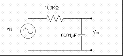
- Now we will build Circuit 1. Shut off the function generator and disconnect the alligator clips from the DAC board. Use the schematic diagram in Figure 9.13 to build your circuit.
- Insert each end of a 100KWΩ resistor into the breadboard horizontally (long direction).
- Insert the 0.001µF capacitor into the DAC board vertically. Make sure that one of the two capacitor leads is inserted into the breadboard in the same column as one of the two leads of your resistor.
- Insert the second lead of your capacitor vertically in any pin in rows F-J.
- Now you will insert two wires into the breadboard to connect your circuit to the Virtual Bench Oscilloscope software (via the DAC board). To do this, connect the wire of pin 3 of your DAC board to the breadboard in the same column that your resistor and capacitor share. Insert the wire coming from pin 4 of the DAC board into the breadboard in the same column as the spare lead of your capacitor.
- Connect the red alligator clip from the function generator to left end of the resistor, i.e. the one not connected to the capacitor. Connect the black alligator clip to the bottom lead of the capacitor, i.e. the one not connected to the resistor, and that also has one of the wires connected to it from the DAC board. If you have wired your circuit successfully, the Virtual Bench Oscilloscope software will have a horizontal line across the center of the screen.
- Turn on the function generator. Change the frequency on the function generator in this pattern (10, 20, 50, 100, 200, 500, 1000, 2000, 5000, 10000Hz) and record the Vp-p reading at each frequency for a total of 10 measurements. Looking at your results, you will see voltages above and below the -3dB point voltage. Now find the- 3dB point exactly by starting with the frequency just below the -3dB point, and then increasing the frequency until you have the voltage corresponding to the -3dB point. Note the frequency and write it down. This is the cutoff frequency.
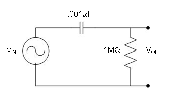
- Shut off the function generator and disconnect the all the wires, capacitors, and resistors from the breadboard. Use the schematic diagram in Figure 9.14 to build Circuit 2.
- Insert two wires into the breadboard to connect your circuit to the Virtual Bench Oscilloscope software (via the DAC board). Connect the wire of pin 3 of your DAC board to the breadboard in the same column that your resistor and capacitor share. Insert the wire coming from pin 4 of the DAC board into the breadboard in the same column as the spare lead of your resistor.
- Connect the red alligator clip from the function generator to left end of the resistor, i.e. the one not connected to the capacitor. Connect the black alligator clip to the bottom lead of the capacitor, i.e. the one not connected to the resistor, and that also has one of the wires connected to it from the DAC board. If you have wired your circuit successfully, the Virtual Bench Oscilloscope software will have a horizontal line across the center of the screen.
- Turn on the function generator. Change the frequency on the function generator in this pattern (10, 20, 50, 100, 200, 500, 1000, 2000, 5000, 10000Hz) and record the Vp-p reading at each frequency for a total of 10 measurements. Looking at your results, you will see voltages above and below the -3dB point voltage. Now find the -3dB point exactly by starting with the frequency just below the -3dB point, and then increasing the frequency until you have the voltage corresponding to the -3dB point. Note the frequency and write it down. This is the cutoff frequency.
- Shut off the function generator and disconnect the all the wires, capacitors, and resistors from the breadboard. Use the schematic diagram in Figure 9.15 to build Circuit 3. Note that the circuit is symmetrical, and that both the input and output of the circuit are connected to the two ends of the inductor and capacitor.
- Insert two wires into the breadboard to connect your circuit to the Virtual Bench Oscilloscope software (via the DAC board). Connect the wire of pin 3 of your DAC board to the breadboard in one of columns that your inductor and capacitor share. Insert the wire coming from pin 4 of the DAC board into the breadboard in the other column shared by the inductor and capacitor.
- Connect the red alligator clip from the function generator to the top lead of the capacitor. Connect the black alligator clip to the bottom lead of the capacitor. If you have wired your circuit successfully, the Virtual Oscilloscope software will have a horizontal line across the center of the screen.
- Turn on the function generator. This circuit
requires a slightly different setup. Sweep through the frequencies on the
function generator, and you will see that the output voltage varies, with a
peak around 500Hz. Find the frequency where the voltage is a peak, and note the
peak to peak voltage as well. This voltage will probably be very low.
Increase the input voltage on the function generator until the peak to voltage
is 2 Volts. This might require an input voltage from the funcation generator as high as
20 Volts. It might not be possible to get a 2.0V output. If this happens, record the highest
voltage you can get and use that instead for the input voltage.
Once you have the 2 Volts peak to peak on the oscilloscope, use this voltage as VIN in your calculations rather than the voltage you used earlier. Multiply this voltage by .707 so you can find the two -3dB points.
- Change the frequency on the function generator in this pattern (10, 20, 50, 100, 200, 500, 1000, 2000, 5000, 10000Hz) and record the Vp-p reading at each frequency for a total of 10 measurements. Looking at your results, you will see voltages above and below the two -3dB point voltages. Now find each of the -3dB points exactly by starting with the frequency just below the -3dB point, and then increasing the frequency until you have the voltage corresponding to the -3dB point. Note the frequency and write it down. This is the cutoff frequency.
- Shut off the function generator and disconnect the all the wires, capacitors, and resistors from the breadboard. You have now completed the lab.
- Create three tables in Microsoft Excel (one for each circuit) to record your data. Remember your VIN is a constant. Each table should look like Figure 9.16.
- Instruct Microsoft Excel to calculate the gain using this equation:
- Plot three Frequency (X) vs. Gain(Y) graphs using the X,Y Scatter template. Make one graph for each circuit.
- Change the x-axis to logarithmic scale. To do this, right-click on the x-axis and select Format Axis. Click on the Scale tab and check the Logarithmic Scale checkbox. Click OK.
- Identify each of the three circuits as a low-, high-, or band-pass filter. If it’s a high pass or low pass filter, find the -3dB point and the cutoff frequency.
Figure 9.12: The Virtual Bench Oscilloscope program window
Warning: Do not touch the Amplitude or Duty knobs for first two circuits. If you do, you will have to recalibrate both the function generator and the Virtual Bench Oscilloscope.
Figure 9.13: Circuit 1 (R = 100KΩ, C = 0.0001µF)
Figure 9.14: Circuit 2 (R = 1 MΩ, C = 0.001µF).
Figure 9.15: Circuit 3 (C = 100µF, L = 1mH)
Note: At this point you will be changing the voltage on the signal generator for the first time since the start of the lab. However, once you have changed the voltage with the next step, do not change the voltage again for the rest of the lab or you will have to restart from the next step forward.
Data Analysis
|
Frequency (Hz) |
VIN (Volts) |
VOUT (Volts) |
Gain=20log(VOUT/VIN) (dB) |
|
10 |
2.0 |
|
|
|
20 |
2.0 |
|
|
|
50 |
2.0 |
|
|
|
100 |
2.0 |
|
|
|
200 |
2.0 |
|
|
|
500 |
2.0 |
|
|
|
1000 |
2.0 |
|
|
|
2000 |
2.0 |
|
|
|
5000 |
2.0 |
|
|
|
10000 |
2.0 |
|
|
Your lab work is now complete. Please clean up your workstation. Return all unused materials to your TA. Refer to section 9.3 Your Assignment for the instructions you need to prepare your lab report.
