Digital Logic
Objective
The experimental objective of this lab is to design a combinational logic circuit for a given problem statement, and to activate it under specific conditions and test it using LabVIEW. After testing, it will be built on an NI-ELVIS II+ prototyping board.
Overview
The first step in understanding the digital circuits that control the function of electronic devices is the mastery of Boolean logic. George Boole, an English mathematician, established modern symbolic logic in 1854 with the publication of his paper, "Laws of Thought." Boolean logic is the foundation of digital circuitry. Boole's method of logical inference allows conclusions to be drawn from any proposition involving any number of terms. Boolean logic demonstrates that the conclusions found are logically contained in the original premises (Encyclopedia Britannica, 2003).
Truth Tables
In Boolean logic, there are only two values, true and false, represented by the numbers 1 and 0, respectively. These values are combined in equations to yield results that also have these two values. The equations are represented by truth tables that show the inputs to the equation and the outputs produced for those inputs. The rows of the table contain all the possible combinations of 1s and 0s for the inputs. The number of rows is determined by the number of possible combinations.
To illustrate a truth table and additional concepts that will be introduced, an example problem statement will be given. Think of an ATM that has three options: print a statement, withdraw money, or deposit money. The ATM will charge a fee to (1) withdraw money or (2) print a statement without depositing money. The intent of the problem is to develop a Boolean equation and logic circuit that will determine after which possible combination of actions will someone get charged a fee. First, a truth table should be made for all the possible combinations of inputs. The inputs are the ATM's three functions. Let variable stand for printing a statement, for withdrawing money, and for depositing money. There is one output, which is whether or not the ATM will charge a fee. The output will be denoted by . The truth table in Table 1 shows all the possible combinations of the inputs and their corresponding outputs.
 stand for printing a statement,
  for withdrawing money, and
  for depositing money. There is one output, which is whether or not the ATM will charge a fee. The output will be denoted by
  . The truth table in Table 1 shows all the possible combinations of the inputs and their corresponding outputs.
Table 1: Truth Table for the ATM Example
| Inputs | Output | ||
|---|---|---|---|
| 0 | 0 | 0 | 0 |
| 0 | 0 | 1 | 0 |
| 0 | 1 | 0 | 1 |
| 0 | 1 | 1 | 1 |
| 1 | 0 | 0 | 1 |
| 1 | 0 | 1 | 0 |
| 1 | 1 | 0 | 1 |
| 1 | 1 | 1 | 1 |
Logic Gates
Boolean logic is applied to digital circuitry through the use of simple logic gates. There are symbols for each of these gates, and the connections between them are represented by lines running from the output of one gate to the input of another. A line can connect only one output to each input. There are seven of these gates: the NOT, AND, OR, NAND, NOR, XOR, and XNOR gates. Only the first three will be used in this lab (Figure 1).

The NOT gate is the simplest of these three. It is an inverter. It has one input and produces its opposite as the output. For example, if a 1 value is put into a NOT gate, a 0 value is outputted, as seen in Table 2. The symbol for the operation is a horizontal bar over the variable. The truth table for a NOT gate is shown in Table 2.
| 0 | 1 |
| 1 | 0 |


The AND gate performs a multiplication operation on its inputs. If all the inputs are true, the output is also true. But if either of the inputs is false, the output is also false. An AND gate can have two or more inputs, but for this lab, it will have two inputs (denoted by A and B in Table 3). The symbol for the AND operation is a dot (·) or the two inputs one after the other with nothing between them. The truth table for an AND gate is shown in Table 3.
| 0 | 0 | 0 |
| 0 | 1 | 0 |
| 1 | 0 | 0 |
| 1 | 1 | 1 |


An OR gate performs an addition operation on its inputs. If either of the inputs is true, the output is also true. But if all the inputs are false, the output is also false. An OR gate can have two or more inputs, but for this lab, it will have two inputs (denoted by A and B in Table 4). The symbol for the OR operation is a plus (+). The truth table for an OR gate is shown in Table 4.
| 0 | 0 | 0 |
| 0 | 1 | 1 |
| 1 | 0 | 1 |
| 1 | 1 | 1 |

Boolean Equations
A truth table is used to write a Boolean equation for a problem. All the combinations that yield an output of 1 are kept, and the equation is written. This is called a Sum of Products solution. Only the combinations that yield an output of 1 are kept because the Boolean equation intends to represent a quantitative function for when the result will have a value of true (when a fee is charged in the example of the ATM machine). The combinations that yield an output of 0 are essentially discarded because there is no interest in when the result has a false value. The Boolean equation for the ATM example can be seen in Figure 2.

Figure 2: Boolean Equation
For each of the combinations (rows) resulting in true in Table 1, the terms of the Boolean equation are determined by multiplying the variables together (the AND operation). If an input is true, the variable can be used as is; for an input that is false, the variable is inverted using the horizontal bar (the NOT operation). Since the output is true if any of the combinations are true, the equation is formed by using addition operations (the OR operation) on all the terms formed by the product of each combination.
Karnaugh Maps (K-Maps)
A truth table showing every possible combination of inputs and their corresponding outputs yields a Boolean equation that is the solution to a problem in digital logic. However, this equation can be simplified using a Karnaugh map (K-map). A K-map identifies and eliminates all the conditions that do not contribute to the solution. The resulting simplified Boolean equation is used to build the digital circuit and will be a combination of the logic gates described above.
A K-map is a two-dimensional representation of the truth table that shows the common characteristics of the inputs. For an equation with three inputs, usually all the combinations of the first two inputs are shown as four columns and the values for the third input are shown as two rows. For four inputs, all the combinations of the third and fourth inputs are shown as four rows. Only one value can change at a time in adjacent rows or columns. For example, in Table 5, the columns change from 00 to 01 to 11 to 10. Table 5 illustrates the K-map for the ATM example.
| 0 0 | 0 1 | 1 1 | 1 0 | ||
|---|---|---|---|---|---|
| 0 | 0 | 1 | 1 | 1 | |
| 1 | 0 | 1 | 1 | 0 |


Simplified Boolean Equations
To develop the simplified Boolean equation, look for the cells that have the 1 value in common. Look for cells that can physically be boxed together, where the number of cells in the box is a power of 2 (1, 2, 4, or 8 and so on). The boxes are allowed to overlap so the same cells can be used more than once. Look for the biggest boxes first, and keep finding smaller boxes until all the cells with a 1 in them are used. This means that sometimes just single cells will remain at the end. The cells in the K-map for the ATM example can be grouped like what is shown in Figure 3.

In this example, all the cells containing a 1 were covered with two boxes. This means is that if the conditions for either box are true, the output will be true. This also means that the simplified Boolean equation will only have two terms. The term for each box can be determined by observing which variables are constant throughout each cell of that box. For the red box, only remains constant through the four cells. switches from the top row to the bottom row, and switches from the left column to the right column. For the blue box, and remains constant through the two cells, while switches from the left cell to the right cell. The two boxes yield the simplified Boolean equation shown in Figure 4.
 remains constant through the two cells, while
This equation meets the conditions in the truth table in Table 1 and achieves the desired result with the minimum number of logic elements.
Combinational Logic Circuits
Lastly, a combinational logic circuit can be created using the simplified equation. First, a NOT operation is performed on by inputting and outputting through a NOT gate. Then, the and inverted are inputted into an AND gate, as denoted by them being multiplied in Figure 4. Finally, the result of the AND operation between the and inverted and the are inputted into an OR gate, as denoted by the addition function in Figure 4. The final combinational logic circuit can be seen in Figure 5.

Materials and Equipment
- A 7432 IC (4 dual-input OR gates)
- A 7408 IC (4 dual-input AND gates)
- A 7404 IC (6 single-input NOT gates)
- A lab PC with LabVIEW 2019 software
- An NI-ELVIS II+ with prototyping board
- Electrical leads
Problem Statement
Farmer Georgi owns a 350-acre dairy farm in upstate New York. In addition to milk and butter, Farmer Georgi sells fresh eggs at the Union Square Greenmarket in Manhattan. It is imperative that Farmer Georgi protects the hen that produces eggs for his business.
Farmer Georgi has two barns, one hen, and a supply of corn. A fox has been attempting to eat the hen by hiding in a barn. The hen can move freely from one barn to the other. Farmer Georgi sometimes stores corn in one barn and sometimes in the other, but he never stores it in both at the same time. The hen would like to eat the corn and the fox would like to eat the hen. Farmer Georgi needs an alarm system that uses digital logic circuits to protect the hen and the corn. The design should use the fewest logic gates and input variables possible. The alarm will sound if:
- The fox and the hen are in the same barn
- The hen and the corn are in the same barn
Procedure
1. Test the Integrated Circuits (ICs)
Before performing the lab, the integrated circuits (IC) used in wiring the alarm system on the NI-ELVIS board must be tested to determine if they are functioning. If the procedure is completed without verifying that the ICs work, problems may occur in the circuit that require additional time and troubleshooting. The system for checking the ICs uses an Arduino board to send and receive signals from the AND/OR/NOT chips and determines if they are functioning properly.
First, load the chip onto the Arduino board (Figure 6) and start the Serial Monitor on the Arduino program. The code will cycle through the basic inputs (0, 1 for NOT; 00, 01, 10, 11 for AND/OR) and then send the outputs of each gate in the chip back to the Arduino board. The code compares those results to the expected result. It displays each input/output pair and displays the final result indicating if the chip is functional or defective. The goal is to determine if the gates are outputting the correct results. After, remove the chips carefully from the Arduino board.

2. Procedure
- The two barns must be assigned a numeric equivalent before the truth table is prepared. Use 1 for Barn 1 and 0 for Barn 2 (1 does not mean true and 0 does not mean false for the inputs). For the alarm output, use 0 to indicate that the alarm should be off, and 1 to indicate that the alarm should be on.
- On a sheet of Lab Notes paper provided by the TAs, create a truth table that includes the three inputs and one output. Assign the input variables. Include all possible scenarios for the hen, the corn, and the fox.
- Compute the output column. To do this, analyze the three inputs and logically determine if the alarm will sound in each scenario. Place a 1 in the output column if the alarm will sound and a 0 if it will not.
- Note all the combinations that produce a 1 in the output column. Create a Boolean equation from this table that includes each of the inputs that produced a true output.
- Create a K-map. Draw a map that lists all the possible combinations from the Boolean equation. Use the Boolean equation to fill in the 1s and 0s on the K-map.
- Box the pairs of 1s appropriately. The 1s may only be boxed in powers of 2 starting with the largest possible combination and working down to the smallest. The outcomes that do not contribute to the solution are to be discarded.
- This process yields a simplified Boolean equation. Write this simplified Boolean equation down.
- Draw a combinational logic circuit of the simplified Boolean equation.
- Have a TA approve the steps to obtain the combinational logic circuit for accuracy.
- Build the logic circuit in LabVIEW 2019 using the combinational logic circuit that was drawn. Open LabVIEW and select New VI. Go to Window > Tile Left and Right.
- Place three switches on the front panel that represent the hen, the corn, and the fox. Place a Boolean indicator on the front panel to represent the output.
- Go to the Functions palette > Modern tab > Programming > Boolean and select the AND, NOT, and OR gates necessary for the circuit.
- Once the LabVIEW program is complete, have a TA check and approve the circuit.
- Build the circuit on a NI-ELVIS II+ prototyping board. On the board, identify each of the three IC chips as an AND, OR, or NOT gate. To do this, read the number on the chip and match it with the numbers shown in Figure 7. Look for the notch at one end of each chip to orient the chip to the diagrams in Figure 7 and to match the pins.
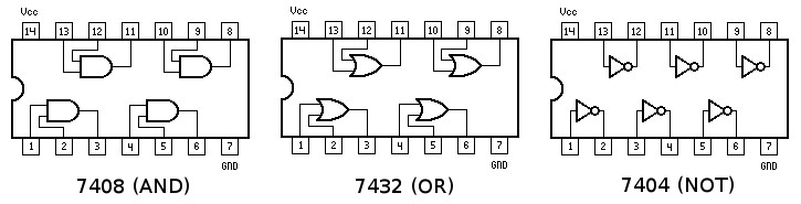 Figure 7: IC Numbers and Pins
- Place the IC chips over the bridge in the NI-ELVIS board (Figure 8).
- Power the chips. Insert one end of an electrical lead into Row 54 (marked +5V) of the NI-ELVIS board. Insert the other end of the lead into Pin 14 of the IC chip. Repeat this process for all three chips.
- Ground the chips using the same method. Insert one end of another electrical lead into Row 53 (marked Ground) of the NI-ELVIS board and the other end into Pin 7 of the IC chip. Repeat this process for all three chips.
- Look at the top right corner of the breadboard to find the Digital Input/Output (DIO) holes. Select one of the DIO rows to use as one of the input variables and begin wiring the circuit based on the simplified Boolean equation. Assign the other DIO rows for the remaining input variables.
- Continue this process until the entire circuit is wired. Insert one end of a lead into the final output of the NI-ELVIS circuit. Attach the other end of the lead to any row for an LED on the board.
- Plug in the NI-ELVIS II+ and connect the USB cable to the lab PC.
- Power on the NI-ELVIS II+ by toggling the switches on the back of the device and top of the device. When the pop-up window appears, select NI-ELVISmx Instrument Launcher and click OK (Figure 9).
- Click on the DigOut Icon on the Instrument Launcher window (Figure 10).
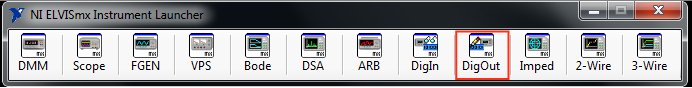 Figure 10: NI ELVISmx Instrument Launcher Dialog Window
- The NI ELVISmx Digital Writer window should appear (Figure 11). Select the appropriate range for the Lines to Write corresponding to the DIO rows used in the wiring. For example, if the fox, hen, and corn are wired to DIO 21, 22, and 23, select 16–23 for the Lines to Write.
- Click Run and toggle the switches corresponding to the fox, hen, and corn. Observe the LED for the alarm light up based on the inputs to each barn.
- Have a TA check the circuit.


The lab work is now complete. Please clean up the workstation. Return all unused materials to a TA.
Assignment
Team Lab Report
Follow the lab report guidelines laid out in the EG1004 Writing Style Guide in the Technical Writing section of the manual. Use the outline below to write this report.
- Describe the problem statement regarding Farmer Georgi
- Describe how AND, OR, and NOT gates work
- Include the truth table, Boolean equation, K-map, simplified Boolean equation, and combinational logic circuit developed during the lab
- What is a truth table? How does it contribute to obtaining a Boolean equation?
- What is a K-map? How does it contribute to obtaining a simplified Boolean equation? To demonstrate the simplification, show what the equation would look like if terms were written for each of the true values and the simplified equation by applying the K-map. Discuss how much simpler the circuitry is as a result of applying the K-map
- Describe how to construct a digital logic circuit using Boolean equations and K-maps
- Explain why the alarm system did or did not work
- Why is there a need for the minimization of a logic design and what are the advantages?
- How does the use of a combinational logic circuit contribute to advances in technology?
- Discuss other possible design/procedural improvements
- Describe how the final combinational logic circuit was obtained
- Include a screenshot of the front and back panels of the LabVIEW VI
Remember: Lab notes must be taken. Experimental details are easily forgotten unless written down. EG1004 Lab Notes paper can be downloaded and printed from the EG1004 Website. Use the lab notes to write the Procedure section of the lab report. At the end of each lab, a TA will scan the lab notes and upload them to the Lab Documents section of the EG1004 Website. One point of extra credit is awarded if the lab notes are attached at the end of the lab report. Keeping careful notes is an essential component of all scientific practice.
Team PowerPoint Presentation
Follow the presentation guidelines laid out in the EG1004 Lab Presentation Format in the Technical Presentations section of the manual. When preparing the presentation, consider the following points.
- How does digital logic impact the world today?
- Looking into the future, how will digital logic change the world?
- Include the truth table, Boolean equation, K-map, simplified Boolean equation, and combinational logic circuit developed during the lab
References
Boole, George, Encyclopedia Britannica, 2003. Encyclopedia Britannica Online. Retrieved July 29, 2003 http://www.britannica.com/eb/article?eu=82823
| ||||||||